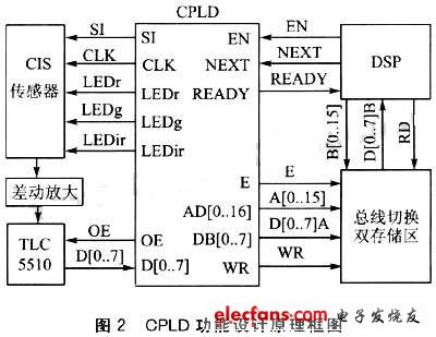
Contact Image Sensor (CIS) is a new type of optocoupler device researched and developed in the 1990s after CCD [1]. It integrates photoelectric sensing array, LED light source array, lenticular lens array, shift register and analog switch in a strip-shaped square box. Its working principle is similar to that of CCD, but compared with CCD, CIS has small volume. The utility model has the advantages of low price, simple structure and convenient installation, and can completely replace the CCD image sensor in the fields of a fax machine, a scanner and a barcode decoder. This paper introduces an image acquisition system based on complex programmable logic device CPLD (Complex Programmable Logic Device) using contact image sensor. 1 System Overview The block diagram of the image acquisition module is shown in Figure 1. Under the control of CPL, the CIS image sensor transmits the gray value of each pixel in the form of analog voltage value through serial shift mode. After signal conditioning by the differential amplifier circuit, the analog voltage is converted into digital by the A/D converter, and the double storage area is rotated by the switching of the bus, and then the converted digital signal is temporarily stored in the memory under the control of the CPLD. In RAM. CPLD is the core component of the system. It mainly performs timing drive of CIS image sensor, control of A/D converter, control of bus switching, generation of address, storage of data and coordination with DSP processor. Bus switching is a key part of the acquisition, and the two-frame rotation structure of image data storage is realized [2]. When the CPLD writes a frame image to the memory RAM1, the DSP reads another frame image to the memory RAM2. When the memory RAM1 is full and the memory RAM2 is read, the CPLD controls the read/write bus to switch to each other, and the CPLD continues to write to the memory RAM2. In the next frame image, the DSP reads the previous frame image from the memory RAM1. The two-frame rotation design method enables the acquisition and processing to be performed simultaneously, improving the efficiency of data acquisition and processing. 2 hardware components 2.1 CIS contact image sensor In the application of this paper, the effective scanning width of the contact image sensor is 216 mm. The photoelectric detecting unit and the lenticular lens are respectively arranged in a line array, and a total of 1728 sensing units can scan the image with three kinds of light sources: red, green and infrared. The clock frequency is 4M Hz and the model number is C2R2166289. 2.2 A/D converter The TLC5510 is a high-speed analog-to-digital converter [3] produced by TI Corporation of the United States. It is an 8-bit high-impedance parallel A/D chip fabricated in a CMOS process with a maximum sampling rate of 20Msps. The TLC5510 not only has high-speed A/D conversion, but also has an internal sample-and-hold circuit, which greatly simplifies the design of the peripheral circuit. With its internal voltage divider resistor, it can be 2V full from the +5V power supply. The reference voltage of the scale. 2.3 CPLD and DSP processor The CPLD chip uses ALtera's MAX7000S series device EPM7128SLC84. This chip can be programmed online by JTAG, with 128 logic macro units and 2500 available logic gates. In the MAX+PLUSII software, the advanced hardware description language programming is used to download the designed hardware logic to the chip, making the hardware design as easy and fast as software design. The buffer memory is composed of two IS61C1024 chips. The IS61C1024 is an 8-bit 128KB high-speed CMOS static RAM with a minimum storage time of 12ns. It can meet the requirements of high-speed data reading and writing, and is also suitable for temporary storage of large-capacity image data. The DSP chip adopts TI's TMS320C5402 chip and adopts the improved Harvard structure, featuring low power consumption and high-speed real-time signal processing. 3 CPLD hardware logic function design CPLD is the core part of image acquisition. It directly controls CIS image sensor and A/D converter to complete digital image data acquisition, conversion and storage, and handshake coordination with DSP processor. The design principle of the overall function of the CPLD module is shown in Figure 2. The CPLD generates the clock signal CLK (4M Hz) of the CIS image sensor, the strobe signal input SI, the red light source strobe LEDr, the green light source strobe signal LEDg, and the infrared light source strobe. LEDir. When the CPLD controls these signals to generate corresponding timings, the CIS sensor serially shifts the gray level of the corresponding pixel to the A/D converter through the analog signal output pin SIG. The CPLD controls the output of the A/D converter to strobe the OE signal, so that the A/D converter can output the converted data. At the same time, the CPLD generates the data storage address AD[0..16] and the write signal WR, which will be A/ The digital image data of the D converter is stored in the corresponding storage area. The bus switching and dual storage area modules realize the rotation of two data storage areas. The schematic diagram is shown in Figure 3. The CPLD controls the storage selection signal E to realize the rotation of the dual storage area. At the initial power-on, the selection is made. The signal E is at a high level, the memory area RAM1 is in a write state, and the RAM 2 is controlled by the DSP processor to change the state of the E to implement bus switching. EN, NEXT, and READY are the handshake signals between the DSP and the CPLD. EN is the enable signal for the CPLD operation. The CPLD starts to work when EN is low. At this time, if a pulse signal is generated on the NEXT end of the DSP processor, the CPLD controls the CIS image sensor to acquire one line (1728 pixels) image. At the same time, READY is set to 0, indicating that the acquisition is in progress. When a line of image acquisition is completed, the READY signal is restored to High level, when EN returns to high level, the CPLD stops working, and the selection signal E is inverted to implement bus switching, and the current memory is switched from the CPLD write state to the DSP read state to realize the rotation of the dual storage area.
Doorbell speaker:
Doorbell speaker is a kind of micro speaker unit which uses a diaphragm made of Mylar material. Doorbell speakers are of ultrathin design and lightweight and clear voice. It is widely used in building security industry (e.g. intercom, video door phone, intelligent door control..)
There are two types of Mylar speakers from the shapes:
1) Round shapes, we have products from 10mm to 57mm in diameter.
2) Oblong shape, we have products in sizes of 1510/1712/1813-..
FAQ
Q1. What is the MOQ? Doorbell Speaker,Doorphone Speaker,Video Doorphone Speaker,Doorbell Wireless Speakers Shenzhen Xuanda Electronics Co., Ltd. , https://www.xdecspeaker.com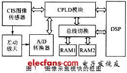


XDEC: 2000pcs for one model.
Q2. What is the delivery lead time?
XDEC: 15 days for normal orders, 10 days for urgent orders.
Q3. What are the payment methods?
XDEC: T/T, PayPal, Western Union, Money Gram.
Q4. Can you offer samples for testing?
XDEC: Yes, we offer free samples.
Q5. How soon can you send samples?
XDEC: We can send samples in 3-5 days.