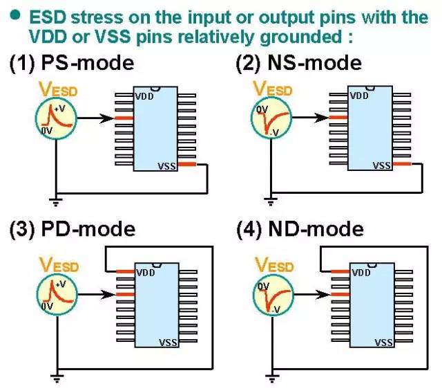
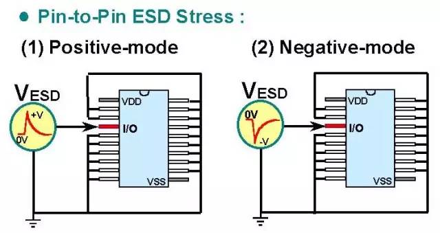
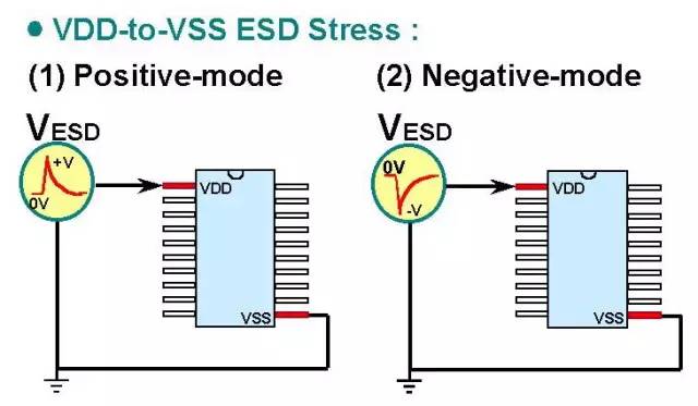
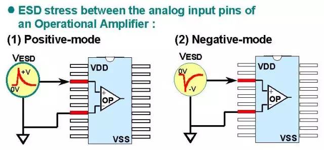
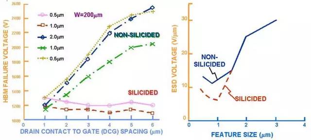
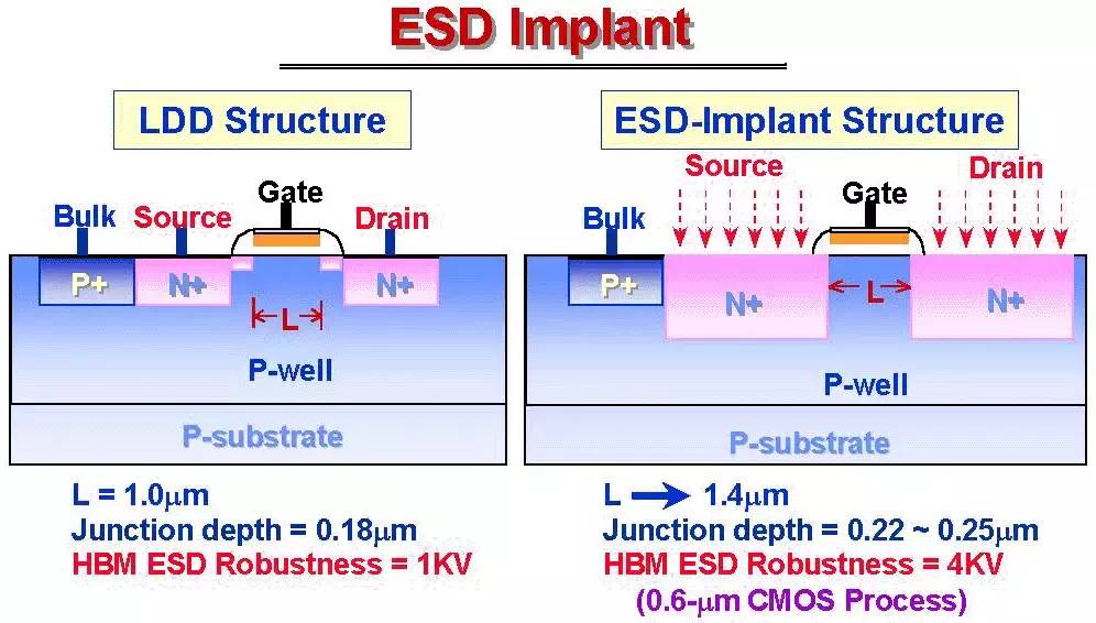
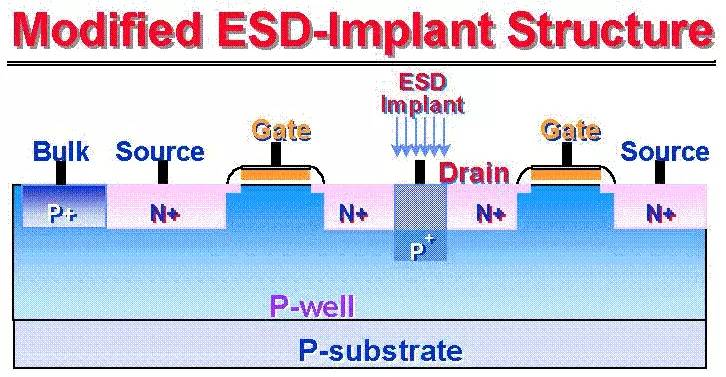
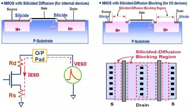
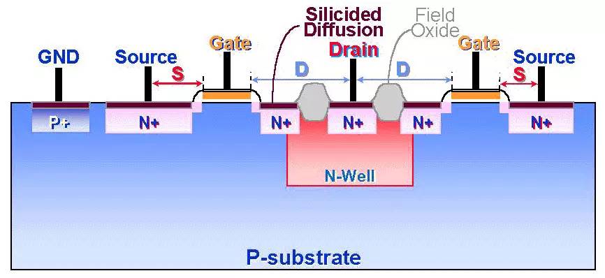
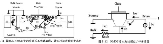
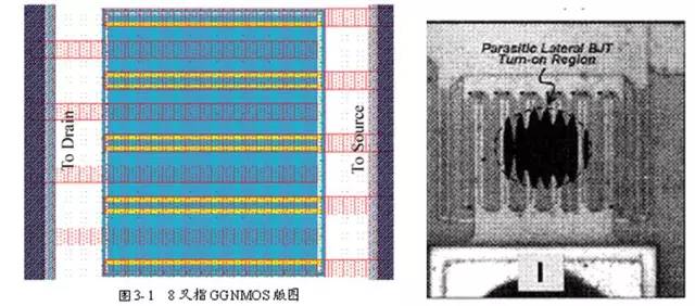
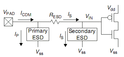
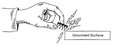
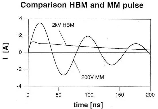
I always wanted to share with you the theory of ESD, which is a fundamental concept in electronics. However, this theory is quite complex, and like any set of rules, it can be interpreted in different ways. Without understanding the basics, trying to draw something as intricate as David from Michelangelo would be impossible. Let’s dive into Electrostatic Discharge (ESD). It's one of the main causes of electrical stress that can damage electronic components or entire integrated circuit systems. Static electricity often carries a very high transient voltage—often exceeding a few thousand volts—which can cause irreversible damage, leading to immediate failure of circuits. That’s why preventing electrostatic damage is a top priority during the design and manufacturing of ICs. Static electricity is commonly generated by humans through activities like production, assembly, testing, storage, and handling. This static charge can accumulate on the human body, equipment, or even components themselves. When an individual unknowingly comes into contact with these charged objects, a discharge path is created, causing electrostatic discharge that can damage sensitive electronics. For example, before working on a computer, it's essential to wear an anti-static wristband to prevent damage to internal chips. Similarly, lightning occurs when a large amount of charge stored in clouds discharges all at once, creating a powerful current. This usually happens on rainy days because higher humidity makes the air more conductive. So, how do we prevent electrostatic discharge? The first step is to reduce static generation at the source, such as minimizing friction, avoiding wool clothing, controlling temperature and humidity, etc. While important, this isn't the focus of today’s discussion. Today, we’re focusing on protecting circuits from external static charges. This is similar to installing a lightning rod for a building—it provides a safe path for excess energy to dissipate without damaging the system. This is a critical concern for many IC designers and manufacturers. Many companies have dedicated teams to develop ESD protection solutions. Today, I’ll explain the basic principles and key concepts behind ESD protection, including PN junctions, diodes, transistors, and snap-back mechanisms. Earlier, we discussed the behavior of a PN junction diode, which conducts in the forward direction and breaks down under reverse bias, known as avalanche breakdown. This property forms the basis of ESD protection. During normal operation, the protection diode remains off. But when static electricity strikes, the diode enters breakdown mode, creating a bypass path that protects the internal circuit or gate. Think of it like a sink drain that prevents water from overflowing by redirecting it away. Now, is the breakdown of the protection circuit permanent? Not necessarily. There are two types of PN junction breakdown: electrical and thermal. Electrical breakdown includes avalanche and Zener effects, both of which are reversible. Thermal breakdown, however, is irreversible and results from excessive heat that melts silicon. Therefore, it’s crucial to control the current during conduction, typically by adding a series resistor to the protection diode. Another interesting point: why is the ESD area not silicided? Because ESD protection must act quickly. The pad on the chip’s input side is where static is first released, not inside the chip. Delaying the release could lead to damage. This is why you often see a diode next to the pad, sometimes with multiple stages for added protection. Before discussing the principles of ESD, let’s cover the standard test methods. According to how static is generated and how it affects circuits, there are four main test modes: Human Body Model (HBM), Machine Model (MM), Charge Device Model (CDM), and Field Induced Model (FIM). In industry, HBM and MM are most commonly used. 1. Human Body Model (HBM): This simulates static charge from a person touching a chip. The industry standard for HBM is MIL-STD-883C method 3015.7, which specifies an equivalent capacitance of 100pF and resistance of 1.5kΩ. The ESD threshold varies by class: Class 1 (less than 2kV), Class 2 (2–4kV), and Class 3 (4–16kV). 2. Machine Model (MM): This models static charge from machines like robots. The equivalent resistance is zero (since it's metal), and the capacitance is still 100pF. Since the resistance is low, the discharge is very fast, and even a 200V discharge can be more dangerous than a 2kV HBM discharge due to the higher current involved. Testing ESD involves applying increasing voltages to specific pins until the device fails. Typically, three tests are performed, starting at 70% of the expected threshold, with steps of 50V or 100V depending on the threshold level. In addition, each chip has multiple pins, so tests are conducted on individual pins or combinations. These include I/O-pin tests, pin-to-pin tests, Vdd-Vss tests, and analog-pin tests. 1. I/O Pins: Each input and output pin is tested separately, with both positive and negative charge scenarios, resulting in four combinations. 2. Pin-to-Pin Test: This involves discharging between two pins, with one pin receiving the ESD voltage while others are grounded. 3. Vdd-Vss Test: Only the power supply pins are tested, with other I/Os floating. 4. Analog Pin Test: This targets differential pairs or operational amplifiers, ensuring they are protected from ESD damage. Now that we’ve covered the principles and testing of ESD, let’s move on to the design process and factors involved. As Moore’s Law continues to drive smaller and more advanced devices, junction depths become shallower, and gate oxide becomes thinner, making ESD damage more likely. The introduction of silicidation also increases ESD vulnerability. As a result, nearly every chip design must address ESD challenges. ESD protection can be addressed either through fabrication process changes or IC layout design. You might notice that some processes include ESD options, or that design rules provide guidelines for ESD protection. Some customers even design ESD based on SPICE models. 1. Process-Level ESD: This involves modifying the PN junction or its load resistance. For example, using non-silicide regions or adding series resistors to increase resistance and improve ESD performance. 1) Source/Drain ESD Implant: LDD structures can create sharp corners that are prone to ESD damage. To mitigate this, deeper implants can be used to round the corners and improve ESD capability. 2) Contact ESD Implant: Adding P+ boron under N+ drains can lower the breakdown voltage, helping protect the gate from ESD damage. 3) SAB (Salicide Block): Blocking silicidation in certain areas increases resistance, improving ESD performance without changing the MOS structure. 4) Series Resistance Method: This approach adds resistance to the ESD path, mimicking the effect of SAB without requiring additional masks. 2. Design-Level ESD: This depends on the designer’s expertise. Some companies provide ESD design rules, while others rely on custom layouts. A common approach is to short the gate, source, and bulk together, and tie the drain to the ESD voltage at the I/O end. For NMOS, the gate is kept off, and the source/bulk junction is shorted. When ESD occurs, the drain/bulk junction breaks down, causing the parasitic lateral NPN transistor to enter the active region, enabling snap-back and providing protection. PMOS works similarly but is generally less prone to snap-back. This principle seems simple, but achieving reliable ESD protection requires careful design. How to trigger BJT? How to maintain snap-back? How to support HBM > 2kV or 4kV? Triggering the BJT requires sufficient substrate current. Multi-finger designs are now common, but they face challenges like reduced gain and uneven triggering across fingers. To overcome this, techniques like SAB or adding inner pickup implants can help. Some key points about snap-back ESD: 3. Gate-Coupled ESD Technology: This addresses the issue of multi-finger uniformity. By coupling the gate voltage, the substrate can be triggered earlier, allowing all fingers to conduct simultaneously, improving overall ESD performance. 4. Complex ESD Protection Circuits: Devices like SCR (Silicon Controlled Rectifier) use parasitic PNPN structures to trigger snap-back and latch-up. While effective, they require careful design to avoid unintended latch-up. Finally, ESD design is highly complex. I’ve only scratched the surface here. The main methods include resistors, diodes, MOS transistors, parasitic BJTs, and SCRs. ESD is not just about design—it’s also deeply tied to the fabrication process. The knowledge is vast, and my understanding is still evolving. Intelligent electronic PCBA,LCD screen driver board,PCBA for home appliances Dongguan Jinglin Communication Technology Co., Ltd. , https://www.jlpcba.com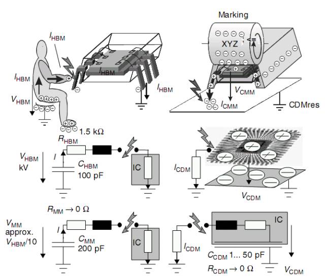
(1). Stress number = 3 Zaps (5 Zaps for worst case) (2). Stress step ΔVESD = 50V(100V) for VZAP ≤1000V; ΔVESD = 100V(250V, 500V) for VZAP > 1000V (3). Starting VZAP = 70% of averaged ESD failure threshold (VESD)