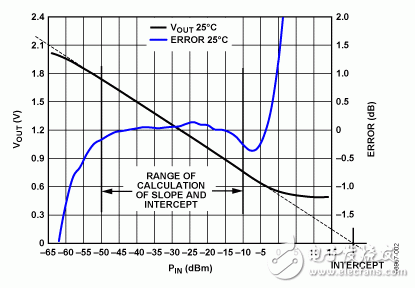
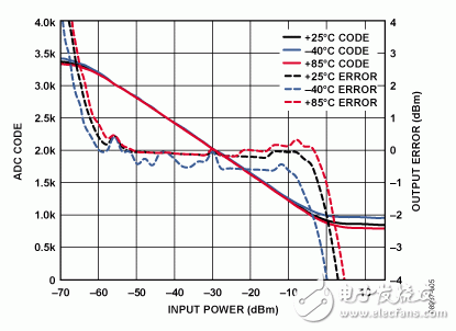
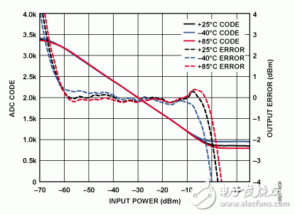
This circuit is used to measure RF power from 1 MHz to 8 GHz with a measurement range of approximately 60 dB. The measurement results are provided as digital codes at the output of a 12-bit ADC with a serial interface and an integrated voltage reference. The output of the RF detector interfaces seamlessly with the ADC and uses most of the input range of the ADC without further adjustment. Perform a simple 2-point system calibration in the digital domain. For 1 MHz to 6 GHz signals, the AD8318 maintains accurate logarithmic consistency and operates up to 8 GHz. The typical input range is 60 dB (re: 50 Ω) with an error of less than ±1 dB. The AD8318 has a response time of 10 ns and is capable of detecting RF bursts above 45 MHz. The device has excellent logarithmic intercept stability (±0.5 dB) over temperature. The AD7887 can be configured for single or dual channel operation through the on-chip control registers. In the default single channel mode, the AD7887 can operate as a read-only ADC, simplifying control logic. The data shown is for two devices operating over the −40°C to +85°C temperature range. Figure 1. Software-calibrated RF measurement system (schematic diagram: decoupling and all connections not shown) The measured RF signal is applied to the AD8318. The device is configured in a so-called "measurement mode" with pin VSET connected to VOUT. In this mode, the output voltage is linearly related to the input signal level (nominally −24 mV/dB) and the typical output voltage range is 0.5 V to 2.1 V. The output of the AD8318 is connected directly to the 12-bit ADC AD7887. The ADC uses its own internal reference and the input range is configured from 0 V to 2.5 V, so the LSB size is 610 μV. When the RF detector provides a nominal slope of −24 mV/dB, the digital resolution is 39.3 LSB/dB. Because of the high resolution, it makes little sense to adjust the 0.5 V to 2.1 V signal from the RF detector so that it fits the ADC's 0 V to 2.5 V range. The transfer function of the detector can be approximated as the following equation: Where SLOPE is the slope in mV/dB (nominal value −24 mV/dB); Intercept is the y-intercept in dBm (nominal 20 dBm); PIN is the input power in dBm. Figure 2 shows a typical relationship between the detector output voltage and the input power. Figure 2. Typical relationship between the output voltage of the AD8318 and the input signal. At the output of the ADC, the equation can be expressed as: Among them, SLOPE_ADC is the code number / dBm, PIN and Intercept are expressed in dBm. Figure 3 shows a typical detector power sweep in terms of input power versus observed ADC code. Figure 3. Input = 900 MHz, ADC uses a 2.5 V internal reference Since the slope (SLOPE) and the intercept (Intercept) vary from device to device, system level calibration is required. The calibration method is to apply two known signal levels close to the end of the linear input range of the AD8318 and then measure the corresponding output code of the ADC. The selected calibration point should be fully within the linear operating range of the device. Using two known input power levels (PIN_1 and PIN_2) and the observed corresponding ADC codes (CODE_1 and CODE_2), SLOPE_ADC and Intercept can be calculated by: After calculating and storing SLOPE_ADC and Intercept (stored in non-volatile RAM) during factory calibration, you can use them to calculate the unknown input power level PIN when working in the field by: Note that the calibration points used for the data shown are −50 dBm and −10 dBm. It also shows the difference between the transfer function of the AD8318 RF detector and the above equation, especially at the end of the transfer function. This difference (in dB) can be expressed as: Where CODE_OUT is the ADC output code; SLOPE_ADC is the stored ADC slope in units of code/dBm; Intercept is the stored slope; PIN_TRUE is the actual input power. Figures 3 through 8 show the system performance that an RF power measurement system can achieve with the AD8318 and AD7887BR. The curve in the figure reflects the relationship between the RF input power (dBm) and the ADC output code and output error (dBm). The data used to generate these curves is measured at various input power levels, frequencies, temperatures, and using an internal or external reference voltage source from the ADC. It can also be seen from these figures that when the ADC uses a low drift external reference, it can improve system performance and reduce drift caused by temperature. See the "Common Changes" section for more details on using an external reference. Figure 4. Input = 900 MHz, ADC uses a 2.5 V external reference Figure 5. Input = 1.9 GHz, ADC uses a 2.5 V internal reference Figure 6. Input = 1.9 GHz, ADC uses a 2.5 V external reference Figure 7. Input = 2.2 GHz, ADC uses a 2.5 V internal reference Figure 8. Input = 2.2 GHz, ADC uses a 2.5 V external reference The test setup consisted of the AD8318-EVALZ and the EVAL-AD7887CBZ with an AD7887BR installed. The two evaluation boards were connected using an SMA to SMB adapter cable and placed in the TestEquity Model 107 environment compartment. Next, connect an evaluation board 2 (ECB2) to the AD7887 evaluation board by testing the slots in the door. ECB2 is used to provide power and to send, receive, and collect serial data from the AD7887 evaluation board. The ECB2 parallel port is connected to the expansion jack of a laptop. This notebook is used to load, run, and view the AD7887 evaluation software on ECB2. The RF input signal required for the AD8318 evaluation board is generated using the Rhode & Schwartz SMT-03 RF signal source. The AD8318 is powered from the Agilent E3631A supply and produces an external reference for the AD7887 ADC. For more information on board configuration, please refer to the AD7887 evaluation board schematic. The AD7887 is a dual, 12-bit ADC with an SPI interface. If the final application requires only one channel, the 12-bit AD7495 can be used. In multi-channel applications that require multiple ADC and DAC channels, the AD7294 can be used. In addition to providing four 12-bit DAC outputs, this subsystem chip also contains four non-dedicated ADC channels, two high-side current sense inputs, and three temperature sensors. Current and temperature measurements are digitally converted and can be read via an I2C compatible interface. The temperature stability of the circuit can be improved with an external ADC reference. The AD7887's 2.5 V internal reference has a 50 ppm/°C drift and drifts approximately 15 mV over a 125°C temperature range. The detector's slope is −24 mV/dB, so the ADC reference voltage drift will contribute approximately ±0.3 dB to the expected temperature drift error. The temperature drift of the AD8318 is approximately ±0.5 dB over a similar temperature range (depending on frequency, see the AD8318 data sheet for details). If an external reference is used, it is recommended to consider the 2.5 V reference ADR421. It has a temperature drift of 1 ppm/°C; in the −40°C to +85°C range, the reference voltage varies by only 312 μV, which has negligible effect on the overall temperature stability of the system. If the dynamic range requirements are low, the AD8317 (55 dB) or AD8319 (45 dB) log detector can be used. Floating Ball Liquid Level Sensor The floating ball liquid level transmitter is composed of magnetic floating ball, measuring conduit, signal unit, electronic unit, junction box and mounting parts. Generally, the specific gravity of the magnetic floating ball is less than 0.5, which can float above the liquid level and move up and down along the measuring conduit. The conduit is equipped with measuring elements, which can convert the measured liquid level signal into a resistance signal proportional to the change of liquid level under the action of external magnetism, And convert the electronic unit into 4 ~ 20mA or other standard signal output. Floating Ball Liquid Level Sensor,Liquid Level Measuring Sensor,Float Type Liquid Level Sensor,Liquid Level Measurement Sensor Taizhou Jiabo Instrument Technology Co., Ltd. , https://www.taizhoujiabo.com


![]()
![]()


The liquid level sensor is a modular circuit, which has the advantages of acid resistance, moisture resistance, shock resistance and corrosion resistance. The circuit contains a constant current feedback circuit and an internal protection circuit, which can make the maximum output current no more than 28ma, so it can reliably protect the power supply and prevent the secondary instrument from being damaged.
Software-calibrated 50MHz to 9GHz RF power measurement system built with logarithmic detector AD8318
Circuit function and advantage