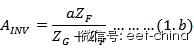
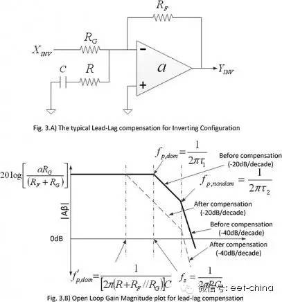
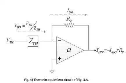
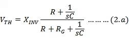
Although op amp compensation is common, it can sometimes be challenging, especially when the requirements and constraints exceed the designer's control, and the designer must choose an optimal compensation technique. Perhaps one of the most challenging reasons is that the general literature focuses more on the differences between different compensation techniques than on similarities. In addition to focusing on conceptual differences, it is also wise to focus on similarities, in order to better understand the close relationship between clearly different technologies and concepts. In order to achieve this goal, this paper first discusses a few of the determining factors of the op amp, and finally gradually transitions to the compensation technology that is often used in the circuit but is rarely understood. This article also briefly introduces the strict definition of the compensation network and focuses on the possible conflicts that appear in the literature. Feed forward gain: Which node is it relative to? Before discussing op amp compensation, it is important to first understand the two most basic configurations of the op amp, namely, in-phase (Figure 1A) and inversion (Figure 1B). A large amount of literature has been introduced on the closed-loop gain of these two configurations, and the difference between closed-loop transfer functions is emphasized. Figure 1A: Typical in-phase configuration. Figure 1B: Typical inverting configuration. Figure 1C: Equivalent in-phase version of the inverted configuration. In order to facilitate the understanding of the difference between the feedforward gains of the two configurations, equations 1.a and 1.b corresponding to the in-phase and inverting configurations, respectively, are given. One might ask why the feed forward gain of the inverting configuration (AINV) is different from the in-phase configuration (ANINV), and in fact the two configurations use the same op amp. Formula 1.a Equation 1.b Let us first look at how similar the two configurations are actually, and then explain why the pure mathematical expressions of the feedforward gain are different. The inverted configuration shown in Figure 1B can be converted to the equivalent in-phase configuration shown in Figure 1C. This conversion is the result of determining the same output as the inverting configuration after determining the input required by the in-phase configuration. 2A and 2B correspond to the block diagram representations of Figs. 1A and 1C, respectively. Note the similarities between Figure 2A and Figure 2B. These two figures show that the two configurations are identical when viewed from the subtraction module to the output. The subtraction module models the subtraction of the two inputs of the op amp. In the reverse-phase configuration block diagram (Figure 2B), the input signal (-XINV) is first multiplied by the ZF/(ZF+ZG) factor and then reaches the input of the subtraction module, named XINV,i. Between the two block diagrams of Figure 2A and Figure 2B, the feedforward gain and feedback factor are exactly the same when strictly observed relative to the subtraction module input or op amp input. The difference between the two configurations is only the input signal when compared to the input signal observation. Mathematical conversion. Therefore, the results of the open-loop gain stability analysis in the two configurations are also the same. The inverse configuration block diagram in Figure 2B can be mapped to Figure 2C by using a linear system processing method. The block diagram in Figure 2C is the result of a simple mathematical process of the inverted configuration, although the sub-modules in Figure 2B better correspond to the elements of the actual physical system. Models that have a better one-to-one correspondence with physical systems are generally easier to understand. 2C is a block diagram representation of the inverted configuration relative to the signal source (-XINV), so the feedforward gain expression (AINV) shown in Equation 1.b appears to be different from the equation 1.a for the in-phase configuration. Expression. Figure 2A: Block diagram of the in-phase configuration. Figure 2B: Block diagram of the inverting configuration. Figure 2C: Reconfiguration block diagram for the inverting configuration. Noise Gain: Not just for noise For ease of understanding, the output noise (including the offset) is usually referenced to the input of the op amp or amplifier. In general, a given polarity of the output voltage is fully referenced to the op amp's positive input, causing the input voltage to have the same polarity as the output voltage, and a full negative input reference can result in an input voltage of opposite polarity. From the perspective of the uncorrelated noise model, the sign or phase of the noise voltage is irrelevant, so the reference of the noise voltage is mathematically equivalent to the inverting or non-inverting input of the op amp. Since the inverting input has a feedback network, the output noise is fully referenced to the op amp's non-inverting input, which quickly yields an efficient and identifiable configuration of the non-inverting amplifier (Figure 1A). Thus, the overall noise gain referenced to either input of the op amp is always equal to the closed-loop gain of the inverting configuration. Therefore, even if an inverting configuration with respect to the signal source is used, the noise referenced to the op amp input actually only sees the in-phase configuration gain equal to (1+ZF/ZG), which is generally called noise gain (NG). ). However, if the noise source is connected to the positive input of the op amp, as in the in-phase configuration, the signal gain and the noise referenced to the input are exactly equal to the noise gain. Compensation technology: There are many kinds of objective op amp compensation techniques, such as “main pole compensationâ€, “gain compensationâ€, “leading compensationâ€, “compensation attenuator†and “lead-lag compensationâ€. The ideal result of any compensation technique is to make the multipole system (higher order system) close to the single pole overall system from a purely stable point of view because the single pole feedback system is unconditionally stable. Most compensation techniques can at least achieve an effective two-pole system state where the second pole (the first non-primary pole) is as far as possible from the first pole (the main pole) and usually has a higher frequency inflection point, and the inflection point Relatively far, the impact on stability is negligible. In some cases, the bandwidth is enhanced by intentionally reducing the distance between the primary and non-primary poles, at which point some high frequency peaks can be observed by the gain frequency response. In many electronic technical literature, perhaps the worst-case explanation for all compensation techniques is the lead-lag compensation technique. Unfortunately, some popular references have errors in the open-loop gain curve and related descriptions of lead-lag compensation, so this article will focus on this. The strict definition or at least a clear definition of the advanced network is that its zero frequency amplitude is lower than the pole, thus giving birth to pure two inflection points. In the case of a hysteresis network, the pole frequency amplitude is lower than the zero point. The lead-lag network is a combination of these two networks. The frequency amplitude of all two inflection frequencies of the leading network is smaller than the frequency amplitude of the lagging network. Similarly, in a lag-lead network, the frequency of the two inflection points of the lag network is smaller than that of the advancing network. Regardless of whether it is a lagging-leading network or a lead-lag network, each network forms four inflection points: two poles and two zeros. Given the overall system and technical constraints, one might use any suitable compensation network to compensate for systems that are inherently and sometimes unchangeable. The selected compensation technique may specifically use the introduced zero to cancel the inherent system pole and vice versa, resulting in a purely lower order system. In this paper, Bode plots with open-loop gain expressions are used for stability analysis and the definitions of poles and zeros are obtained. Lead-lag compensation: The implementation of the lead-lag compensation circuit according to the reference is shown in Figure 3A. For practical and simple purposes, assume that the uncompensated op amp has two intrinsic poles: the main pole (?p, dom) and the first non-primary pole (?p, nondom). Figure 3B shows an open-loop gain amplitude plot where the solid line represents the uncompensated op amp and shows the inherent inflection point of the op amp itself. Figure 3A: Typical lead-lag compensation for an inverted configuration. Figure 3B: Open loop gain amplitude map for lead-lag compensation. Introducing a pole (?'p,dom) and a zero (?z) by introducing lead-lag compensation, the introduced pole (?'p,dom) becomes the new principal pole, the introduced zero (?z ) basically offsets the inherent main pole of the op amp (?p, dom), although Figure 3B shows a perfect offset between ?z and ??p, dom. The corresponding (wrong) diagram shown in this document should be understandable. As with many other compensation techniques, a significant advantage of lead-lag compensation is that the spacing between the formed main and non-primary poles is increased, thereby enhancing stability. However, one might ask why not just advance compensation is applied, and the zero point introduced by the compensation network offsets the first non-primary pole inherent in the op amp. A well-known reason is that lead compensation obviously produces bandwidth limitations, while lead-lag compensation does not. Why does lead-lag compensation not limit bandwidth? The answer to this question is not very clear if it is all visible from the open loop gain curve. Someone may get an answer by analyzing the closed-loop amplification process. For the lead-lag compensation case, another paper well proposes a closed-loop gain calculation formula, but here is an intuitive explanation of why this technique does not limit the bandwidth, although some simple mathematical methods are utilized. In the two amplifier configurations shown in Figure 1, the negative input of the op amp is a negative feedback point, so as long as the open-loop gain amplitude at the frequency of interest is large enough, this is a very low incremental impedance node. Known as virtual land. So it makes sense to convert the source voltage to the equivalent input signal current and then multiply the feedback resistor value (RF) to get the pure output voltage (YINV), as shown in Figure 4. Figure 4: Devin's equivalent circuit of Figure 3A. A popular way to accomplish this conversion is through the Dai Wenning equivalent network. Figure 4 shows the Devinning equivalent circuit of Figure 3A. In Figure 3A, it is assumed that the op amp and its feedback network are not present, in other words the load is removed, and then the contribution from the input source (XINV) at the negative input of the previously connected op amp is considered. This contribution can be referred to as the Dai Wenning equivalent voltage (VTH), whose amplitude decreases with increasing frequency because the impedance of the compensation capacitor decreases as the frequency increases. At the same time, due to the effect of the compensation capacitor, Dai Wenning's equivalent series impedance (ZTH) is affected by the same method. Therefore, the net signal current (ISIG) flowing to the negative input of the op amp (virtual ground) will be equal to (VTH/ZTH=XINV/RG), where all inflection points in the molecular term VTH will be offset by all inflection points in the denominator ZTH. This in turn results in a signal current that is unaffected by the compensation network. Eventually there is no bandwidth limitation due to the use of lead-lag networks. See Equation 2a and Equation 2b.
ZGAR FILTER TIP
ZGAR electronic cigarette uses high-tech R&D, food grade disposable pod device and high-quality raw material. All package designs are Original IP. Our designer team is from Hong Kong. We have very high requirements for product quality, flavors taste and packaging design. The E-liquid is imported, materials are food grade, and assembly plant is medical-grade dust-free workshops.
Our products include disposable e-cigarettes, rechargeable e-cigarettes, rechargreable disposable vape pen, and various of flavors of cigarette cartridges. From 600puffs to 5000puffs, ZGAR bar Disposable offer high-tech R&D, E-cigarette improves battery capacity, We offer various of flavors and support customization. And printing designs can be customized. We have our own professional team and competitive quotations for any OEM or ODM works.
We supply OEM rechargeable disposable vape pen,OEM disposable electronic cigarette,ODM disposable vape pen,ODM disposable electronic cigarette,OEM/ODM vape pen e-cigarette,OEM/ODM atomizer device.
Vape Filter Tip,Disposable Pod Vape,Disposable Vape Pen,Disposable E-Cigarette,Electronic Cigarette,OEM vape pen,OEM electronic cigarette. ZGAR INTERNATIONAL(HK)CO., LIMITED , https://www.oemvape-pen.com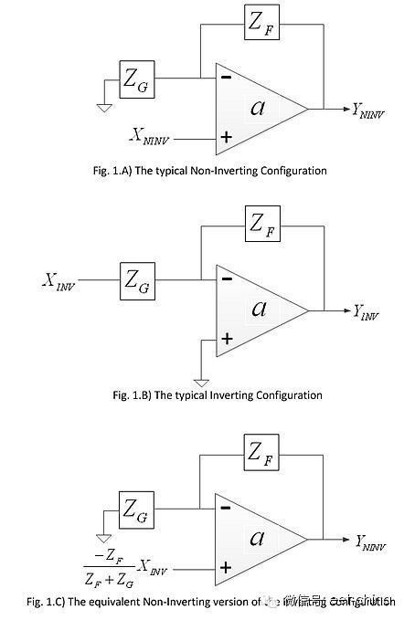


Leading compensation: Different implementations The lead-lag compensation discussed in this discussion (Figure 3A) is implemented by connecting series resistors and capacitors between the negative input of the op amp and ground, or equivalently between the two inputs of the op amp. element. However, when such a series structure is connected between the input-output pins of the amplifying transistor, the compensation technique is referred to as a combination of lead compensation and final pole separation compensation. This series resistance and capacitance compensation structure is almost always present inside the op amp. Usually this process begins by placing a capacitor between the gain cells, which results in pole separation compensation due to the capacitance Miller effect. Then in order to compensate for the right half-plane zero formed, it is necessary to add a series resistor and adjust the resistance to achieve lead compensation. At this time, it is necessary to move the zero point until it cancels the first non-primary pole. Ultimately how people connect such a series resistor and capacitor network depends on the specific requirements and available options of the lead or lead-lag compensation vertex. In order to achieve lead compensation in an amplifier using an op amp IC, a parallel feedback resistor is required to place a feedback capacitor [1, 3]. Although it is an implementation of lead compensation, its intent is usually to offset a pole by introducing a zero point through the compensation network, and is generally the first non-primary pole of the system to be compensated. Concluding remarks According to the strict definition of the compensation network described in the literature, the so-called lead-lag compensation shown in Fig. 3A is strictly a kind of lag compensation. Similarly, the so-called advanced compensation network placed between the transistor amplification nodes is strictly a hysteresis compensation network. This once again reminds people how similar these compensation techniques are actually, and is divided into different categories for different reasons in different references. Perhaps in addition to the "gain compensation" technique, all of the compensation techniques mentioned above can be classified as "knee compensation" techniques because the DC open-loop gain amplitude remains constant during the compensation process, and only the inflection point undergoes repositioning, creation, and elimination. The process of combining.
