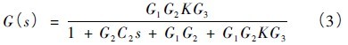
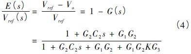
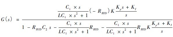
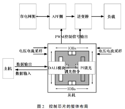
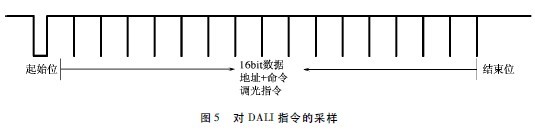
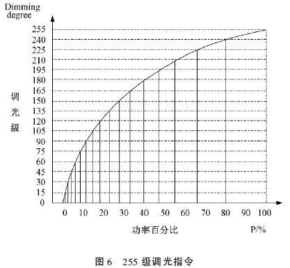
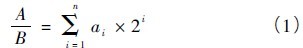
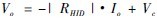
1 Introduction As a new type of energy-saving electric light source, HID lamps have attracted wide attention due to their high efficiency, energy saving, good color rendering and long life. The HID lamp has a negative resistance characteristic when it works, and needs ballast to perform impedance compensation. In addition, the impedance of the HID lamp changes greatly from startup to stable operation, and the HID lamp needs constant current regulation at startup, in transient and steady state. Constant power control is provided to provide impedance matching for the lamp at different stages. HID lamps produce acoustic resonances when operating at high frequencies, usually with low frequency square waves. The traditional low-frequency square wave adopts the analog control method, which has the advantages of high speed and high precision, but the overall reliability of the device is low. The improved digital control method has higher reliability than the analog method, but the control precision is much lower. Therefore, these two control strategies currently have certain defects. In addition, in order to solve the problem of digitalization and network realization of electronic ballasts, a prototype of a new control strategy is sought, which requires a powerful device for hardware support. According to the requirements of various aspects, this paper designs the DALI communication protocol stack based on the FPGA hardware platform, which provides a complete communication interface and a communication protocol codec platform that can be directly called by the user for the design of the networked ballast. Digital PID control module for bridge HID lamp constant current and constant power inverter function. Because FPGA has the advantages of high precision, high speed, good reliability, and low price of the film, it can improve the defects that the HID lamp ballast cannot be balanced in reliability, precision and control speed. Finally, the experimental verification shows that the control chip has complete functions, high constant current and constant power control accuracy, fast response, and the control strategy is more flexible, accurate and reliable, and realizes remote networked lighting control through DALI bus. 2 full digital HID ballast circuit structure As shown in Figure 1, the HID electronic ballast converts the commercial 220V to DC bus voltage 311V through the rectifier bridge, and then passes it to the full-bridge inverter circuit through the active power factor correction circuit APFC, and finally realizes the HID lamp through the filter component. powered by. The control chip mainly plays the role of collecting current and voltage signals and controlling the switching tubes of the APFC circuit and the inverter circuit. In modern lighting, communication with the ballast is required to feedback the HID lamp status and control dimming, so the control chip also needs to be integrated into the communication protocol. 3 Digital Control Strategy As shown in Figure 2, the controller first obtains instructions from the host through the DALI module, and performs ballast setting, dimming, or feedback control according to the instructions. The DALI module integrates the digital addressable lighting interface protocol, and sends the data to the PI control module after processing the instruction or feedbacks the current HID lamp electrical status according to the value HID collected by the PI control module. The PI module communicates with the DALI module to receive the dimming command of the DALI module. The current and voltage values ​​of the HID lamp are collected and fed back to the DALI module, and the PWM driving signal is sent to the APFC circuit and the inverter bridge. 3. 1 Design of Digital Addressable Lighting Interface (DALI) Module In order to form a digital communication interface, the design incorporates the DALI protocol into the control chip. As shown in Figure 3, the DALI protocol design slave function can be divided into four parts: DALI protocol reception, processing, power data transmission and status feedback. The DALI module receives RS232, detects the start bit signal, verifies and receives it frame by frame, and then performs data processing according to the register instruction table. After the processing is completed, it sends back data information to the host or sends dimming to the PI module. The operation of the data. The status flow chart is shown in Figure 4. The process implementation methods are as follows: (1) The receiving process follows the Manchester encoding to receive data. “The rising edge jump data is 1, the falling edge jump data is 0â€, and the data packet has 19bit data, as shown in Figure 5, including a rising edge start bit, 16bit valid data, and 2bit high level stop bit. If an error occurs in data reception, it will return again, notify the host and wait for re-reception; if it is correct, the valid data will be stored in the memory. (2) The processing link performs different steps corresponding to the input of different DALI instructions, and can be divided into three types: dimming, setting and query. In the dimming step, the host sends a dimming command to the controller, and the dimming value divides the power into 255 dimming levels by a logarithmic curve. By storing the power data corresponding to each dimming level, the corresponding output is obtained by looking up the table. ,As shown in Figure 6. In the setup step, the controller communicates with the host at the beginning, and the host generates a blank address to the controller to set the address of the HID lamp ballast. During control, the host can control up to 64 HID lamp ballasts by means of "broadcast addressing" for overall control or control of one of the controllers. The valid data received by the receiving host contains 8 bit address bits and 8 bit data bits: "AAAAAAAA + DDDD DDDD". In the query step, the DALI module obtains the current and voltage values ​​from the PI control module, and in conjunction with the dimming value, the operating state of the lamp can be transmitted to the host. (3) The dimming step in the processing step corresponding to the transmission link, the dimming command is sent to the PI module, and the steady-state constant power adjustment is performed on the HID lamp. Since dimming is divided into different methods such as step-by-step dimming or instantaneous dimming, in order to transfer the reference voltage value to the PI module, calculations including 20-bit division are required. In order to reduce the computing resources of the FPGA, the division uses the bit removal method to calculate, and the quotient (retained integer) is regarded as the cumulative sum of the product of the power of 2 and its corresponding coefficient ai. The principle of the algorithm is as follows: The divisor is shifted successively, and compared with the divisor, the coefficients ai are obtained. This design ensures calculation speed and simplifies the resources required for design. (4) The status feedback link corresponds to the inquiry step, and mainly sends the electronic ballast status and the HID light status to the host, and whether the current dimming level and the HID light are on. 3. 2 PI control module design Constant current constant power control for HID lamps requires the design of a PI controller (the PWM control using the DC/DC section to implement the PFC function is no different from the traditional control method, and is not the focus here, not to be elaborated). Taking steady state as an example, first, A/D sampling uses the sampling resistor and current sensor to collect data from the full-bridge inverter circuit to obtain 10-bit digital quantities Io and Vo, respectively. According to the dimming command sent by the host, the reference power data Po is obtained by the look-up table, divided by the sample value Io, and the reference current value Vref is obtained, and the duty ratio is obtained by comparing the Vref and Vo through the comparator and the PI link to achieve constant power adjustment. The constant power modeling of the PI control module is as follows: G3 represents the transfer function of the controller, K is the inverter gain, G1 is the current-voltage characteristic transfer function of the filter element, G2 is the impedance transfer function of the HID lamp, and H1 is the current-voltage characteristic function of the capacitor C2, H2 and H3 It is a voltage feedback function. The control chip receives the dimming command of the host through the DALI module, looks up the table or calculates (for the stepless dimming function), obtains the dimming power control data Pref of the HID lamp, and then inputs the power data Pref into the control unit to obtain the joint sampling result. The current current value Io is calculated to obtain a reference voltage value Vref, which is subjected to adjustment control after passing through the comparator, filtered out from the converter, and finally supplied with energy to the load. According to the Mason formula, the transfer function is Where H2 and H3 can be simplified to 1; G2(s) is the current-voltage characteristic fitting relationship of the HID lamp. The steady-state HID lamp operates in the arc discharge area. Therefore, it can be considered that there is a large negative resistance characteristic, that is, In the absence of PI, Therefore the error to input ratio is Assuming the input is a unit step signal, the small formula 2 = 1 / ( 1 + G1G2KG3) can effectively reduce the steady-state error when G3 is a PI module. The transfer function of the PI Control Module is as follows: 


 . Simplified later