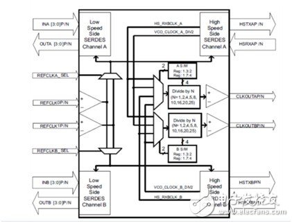
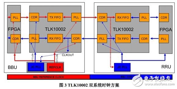
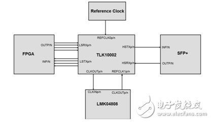
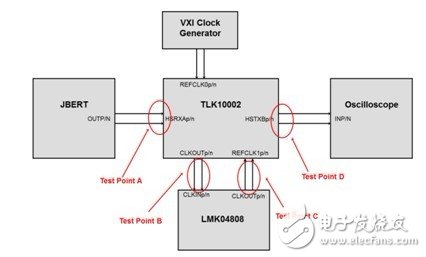
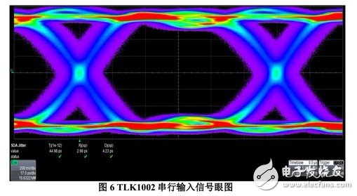
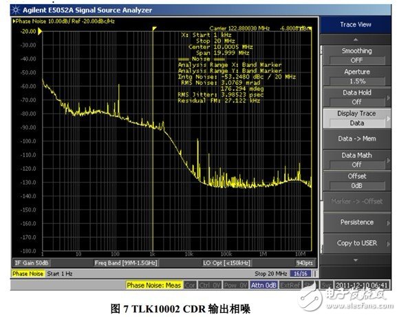
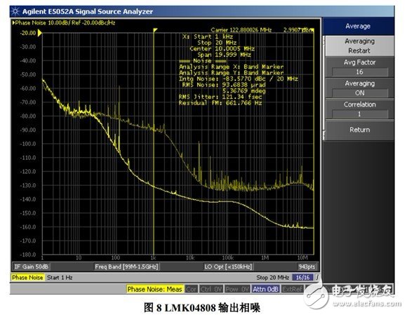
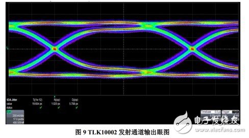
Summary In a distributed base station system, the RRU usually remotely interconnects with the BBU through fiber-optic remote access. Due to the characteristics of the fiber itself, jitter and drift are inevitably introduced during transmission; especially drift, due to its low frequency characteristics, and difficult to filter out, the FIFO may overflow due to insufficient FIFO depth of the SERDES. This article will firstly analyze this problem in general. Based on this, we will use Texas Instruments 10G SERDES device TLK10002 as an example to propose a new solution, which provides the SERDES system clock in dual clock mode, and explores this The specific implementation of the mode. At the same time, in order to verify the feasibility of the dual clock scheme, we built the corresponding test platform and gave the corresponding test results. 1. Analysis of SERDES FIFO overflow caused by fiber drift 1.1 Causes of drift and drift formation Drift is the non-cumulative deviation of the effective moment of a digital signal that deviates from its ideal position in time. The so-called "long-term deviation" refers to a deviation from a slower change over time, and it is generally considered that a frequency of change below 10 Hz is a slower change. The phase noise of the actual digital signal, the high-frequency component of the phase noise during jitter, and the drift are the low-frequency components of the phase noise. In engineering, the high and low frequencies are divided by 10 Hz. The mechanism by which these two frequency components are produced is different. The main reason for the generation of low-frequency components, that is, drift, is the variation of transmission delay in the transmission medium and equipment. For example, the fiber is heated and heated during the day, the delay is increased, the signal is late, and the phase is delayed; the fiber is coldened at night and the delay is reduced. The signal is early and the phase is ahead. The main cause of high-frequency components, that is, the generation of jitter, is the random variation of the zero-crossing of the signal caused by internal noise, such as the phase noise of the oscillator output signal and the uncertainty of the digital logic switching moment. Drift does not directly cause transmission errors, because the recovery clock circuit of the transmission device can track slow changes in phase. Although the drift amplitude changes slowly, the long-term cumulative amplitude may be as high as 1000 UI [3]. 1.2 Analysis of SERDES FIFO overflow caused by drift A typical BBU and RRU system cascading scheme is shown in Figure 1. On the RRU side, since the JC PLL (main clock chip) automatically tracks the incoming serial data stream, the JC PLL adjusts when the input frequency changes. The output frequency is matched to the change in the input frequency. At this instant of the transition, if the read/write rates of the FIFOs of the SERDES may be inconsistent, the FIFO conflicts, causing an overflow. However, this overflow is completely avoidable by selecting a JC PLL that is fast enough to hop, and once the JC PLL is locked to the input data stream and the FIFO reads and writes at the same rate, there is no overflow problem. On the BBU side, it is worth noting the jitter of the clock signal, especially the FIFO overflow caused by drift. If this drift comes from the BBU's own reference clock, since the input data rate is matched to the BBU rate, it will not cause any problems; however, as explained in the previous section, the temperature drift of the fiber may introduce new drift. If the RX FIFOs work in different clock domains on both sides, this fiber introduction drift will cause the SERDES internal FIFO to collide. If the depth of the FIFO itself is insufficient to absorb this collision, it will cause FIFO overflow. 2, BBU SERDES dual system clock scheme and specific implementation 2.1 TLK10002 internal clock architecture The TLK10002 is a dual-channel 10G SERDES chip from Texas Instruments that supports all current CPRI and OBSAI rates from 1.2288Gbps to 9.8304Gbps, making it ideal for wireless base station applications. The internal clock architecture of the TLK10002 is shown in Figure 2. Its A/B channel can provide a reference clock through the REFCLK0P/N or REFCLK1P/N pins. These two reference clocks can be selected via MDIO or REFCLKA_SEL and REFCLKB_SEL pins. achieve. The CDR of the high-speed side SERDES is mainly used to recover the clock signal from the input serial data, and the recovered clock signal is output from CLKOUTAP/N and CLKOUTBP/N. There are several options for the output signal frequency: by register configuration, divide the recovered clock frequency by 1, 2, 4, 5, 8, 10, 16, 20, or 25. For each channel, the high-speed side SERDES and the low-speed side SERDES can operate in one clock domain, ie both use the same reference clock; at the same time, the TLK10002 also provides another clock mode, namely high-speed side SERDES and low-speed side SERDES. Different reference clocks, in this case, the high speed side phase locked loop and the low speed side phase locked loop will work in different clock domains. Figure 2 TLK10002 internal clock architecture 2.2 TLK10002 Dual Clock System Solution The system cascading scheme based on the dual clock TLK10002 is shown in Figure 3. In this scheme, the TLK10002 high-speed side SERDES and low-speed side SERDES use different reference clocks. On the BBU side, the high-speed phase-locked loop uses the local reference clock. Once the high-speed phase-locked loop is locked and a stable link is established between the BBU and the RRU, the CDR of the TLK10002 on the BBU side will have a stable output. The Jitter Cleaner on the BBU provides reference input. Once the Jitter Cleaner is properly locked, its output is used as a reference input for the low-speed side-locked loop. With this configuration, since the SERDES itself can handle frequency offsets of up to 200 ppm, the rates of the transmit and receive channels are completely independent of each other. In this way, both sides of the FIFO work completely in the same clock domain, and there is no risk of overflow in the FIFO. In this case, the FIFO is only used to absorb the phase offset between different clocks and to compensate for the traceability of the jitter cleaner. 2.3 The specific implementation of the dual system clock scheme Take the BBU side as an example. The specific implementation of the dual-system clocking scheme is shown in Figure 4 below. In this scheme, because the LMK04808 has ultra-low phase noise characteristics, we use it as a jitter canceller. Figure 4 Building a BBU SERDES system with a dual clocking scheme For the system shown in Figure 4, the system configuration and operation sequence are as follows: 1) Normally configure the TLK10002 0X00 to 0X0D registers. 2) Wait for the TLK10002 high-speed phase-locked loop HS PLL to lock normally. // As long as the local reference clock is ready, the high-speed phase-locked loop can be locked (this does not require a stable 10G link). 3) Switch TLK10002 ENRX: Set to 0 first, then set to 1. // Make HS SERDES adaptive link status. 4) Wait 10ms. // Wait for the HS SERDES setup parameter to ensure that the CDR provides a valid reference clock for the LMK04808. 5) Configure the LMK04808 to ensure it is properly locked. 6) Wait for the TLK10002 low-speed side phase-locked loop LS PLL to lock normally. / / As long as the LMK04808 is locked and output normally, the LS PLL can be locked normally 7) Restart the data path. //At this time, both the low-speed side and high-speed side SERDES have valid clocks. Restarting the data path optimizes the pointer position of the FIFO and triggers the realignment of the low-speed side Lane. 3, dual system clock program actual test 3.1 Test Setup The TLK10002 dual system clock scheme test setup is shown in Figure 5. J-BERT is used to generate the 9.8304Gbps PRBS7 test signal, which will load 45ps wideband random jitter. The VXI Clock Generator is used to generate the 122.88MHz local clock as the reference clock for the TLK10002 high-speed phase-locked loop; LMK04808 The local Jitter Cleaner uses the default configuration of the LMK04808 evaluation board. The TLK10002 CDR outputs the 122.88MHz signal as the LMK04808 reference input. The LMK04808 outputs the 122.88MHz LVPECL signal as the reference clock for the TLK10002 low-speed phase-locked loop. The TLK10002 is configured for the 9.8304Gbps PRBS test mode. The transmit channel uses the default settings; the high-speed oscilloscope is used to observe the TL30710002 transmit channel output 9.8304Gbps high-speed serial signal. At the four test points A, B, C, and D, we will test the TLK10002 serial input signal eye diagram, TLK10002 recovery clock signal phase noise, LMK04808 output signal phase noise, and TLK10002 transmitter output eye diagram. Figure 5 TLK10002 dual clock system solution test setup 3.2 measured results The TLK10002 serial input signal eye diagram is shown in Figure 6. Its random jitter (Rj) is 2.98ps, the jitter (Dj) is 4.23ps, and the total jitter (Tj) is 44.98ps. Usually, this type of broadband Random jitter is difficult to eliminate by equalization. The TLK10002 recovery clock output phase noise curve is shown in Figure 7. Using the input signal shown in Figure 6, the TLK10002's recovered clock RMS jitter is 3.98ps (1KHz~20MHz). The output phase noise of the LMK04808 is shown in Figure 8. It can be seen that after passing the Jitter Cleaner (LMK04808), the output RMS jitter is only 121fs (1KHz~20MHz) due to the strong jitter cancellation capability of the LMK04808. The TLK10002 transmit channel output eye diagram is shown in Figure 9. The random jitter (Rj) is 1.02ps, the jitter (Dj) is 5.79ps, and the total jitter (Tj) is only 19.6ps. The eye diagram is clear. 4 Conclusion From the above theoretical analysis and actual test results, it can be clearly seen that the dual clock system scheme constructed by TLK10002 and LMK04808 can completely avoid the problem of SERDES FIFO overflow caused by fiber introduction drift; meanwhile, since the transmitter eye diagram is mainly based on local reference The phase noise decision of the clock, this dual clock mode has no effect on the eye diagram and the output noise performance of the transmitter. 1.6 years product warranty (material and workmanship), 25 years module power output warranty
3.Strong framed module, passing mechanical load test of 5400Pa to withstand heavier snow load 4.17% conversion efficiency,reducing installation costs and maximizing the kwh output per unit area.
Polycrystalline Solar Panel,Poly Panel,Poly Solar Panel Yangzhou Beyond Solar Energy Co.,Ltd. , https://www.ckbsolar.com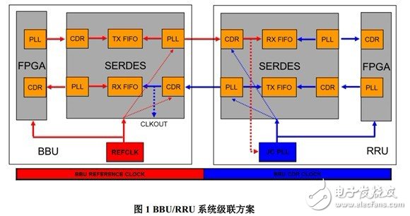
2.Industry leading plus only power tolerance: 0+3%