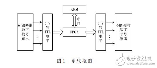
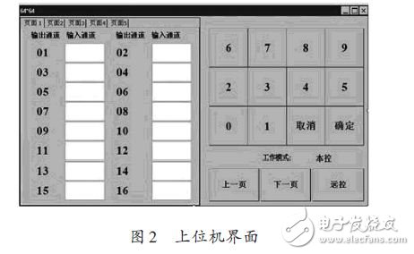
In this paper, FPGA is used as the core component of the control logic. The FPGA-based baseband 64&TImes;64 data distribution matrix design scheme is proposed. The software design idea of ​​the host computer and the internal programming implementation and simulation of the FPGA are introduced. It has been proved that the scheme has the characteristics of large scale, low cost and high speed, and can be widely used in large-scale baseband digital system testing and signal program control distribution scheduling. 0 Preface The data distribution matrix, that is, the matrix switch, as the name implies, refers to a switch product whose structure is arranged in a row and a row. The feature is that each node is connected to one row/column, and each node can be operated separately. Signal routing can be realized by setting different combinations of nodes. . The main advantage of the matrix switch is its simplified line, and the entire test system can easily dynamically change its internal connection path without external manual intervention. The use of matrix switches is very flexible and convenient. It is the most widely used product in program-controlled switch products, and has been widely used in automotive electronics, semiconductor testing, aerospace and other fields. FPGA has the advantages of fast running speed, rich internal logic resources, and a large number of peripheral I/O ports. Therefore, this design uses FPGA as the core device. 1 system structure and function This design is to achieve any cross-over switching of 64-bit input signals to 64-bit outputs, that is, the input and output are in one-to-one correspondence. Since this design is for baseband digital signals, and the crystal frequency selected in the design is 25 MHz, there is no need to consider the problem of FPGA processing asynchronous clock domain data transmission. It only needs to directly convert the corresponding input signal to level conversion. After the code is directly output to the corresponding output interface. The upper computer ARM sends the connection information of the interface to the FPGA through the serial port, and the FPGA decodes according to the received data, and connects the corresponding input with the corresponding output to realize the connection of the specified link. Considering the resources and the number of pins, this design scheme uses Altera's Cyclone III series EP3C25F256 FPGA. Four 32-channel level conversion chips are selected to realize the conversion of 5 V signals to FPGA-recognizable TTL signals. Its structural block diagram is shown in Figure 1. 2 PC design The interface of the host computer is shown in Figure 2. Enter 0~64 in the corresponding input channel text box. After clicking the “OK†button, first compare and judge all the data in the text box. If there is a repetition, an error will be reported, prompting to re-enter. After the error is correct, the connection instructions of 64 interfaces are sent to the FPGA through the serial port in the order of the output interface. Each instruction contains 3 B. The first byte is the information header "AA". If the header byte of an instruction received by the FPGA is not "AA", there is no return information, and the host computer will resend this instruction until Correct so far. The second byte is the input port byte, which is the number in the corresponding text box. If there is no input number, the default is 0. Therefore, if you need to disconnect a link, just enter 0 in the corresponding text box and click OK. Just fine. The third byte is the data corresponding to the output port and is sent in the order of 1 to 64. The "remote control" button in Figure 2 is reserved for use as a computer remote control. Electric Grill,Electric BBQ Grill,Portable Barbecue Grill,Electric Barbecue Shaoxing Haoda Electrical Appliance Co.,Ltd , https://www.zjhaoda.com