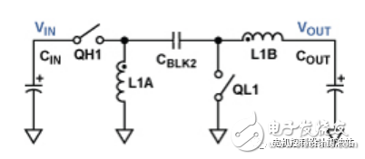
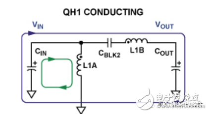
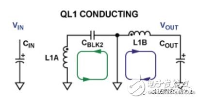
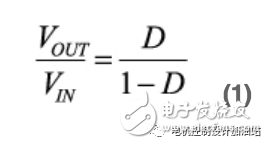
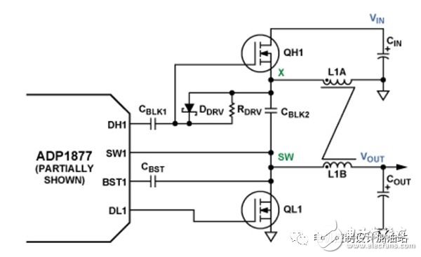
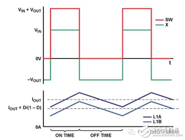
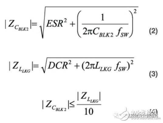
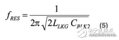
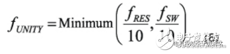
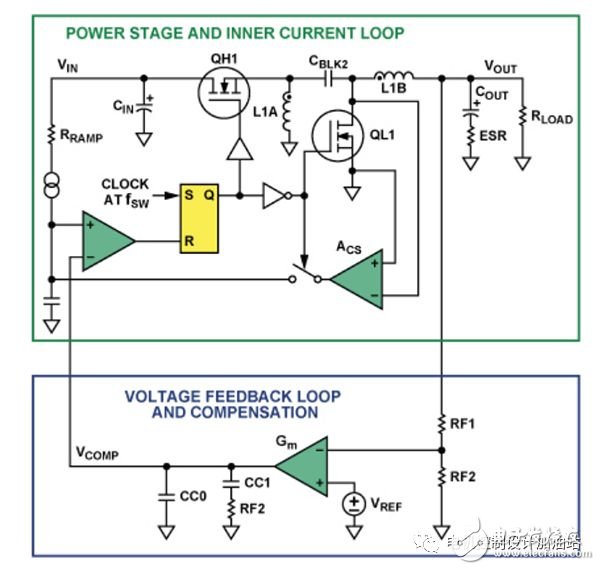
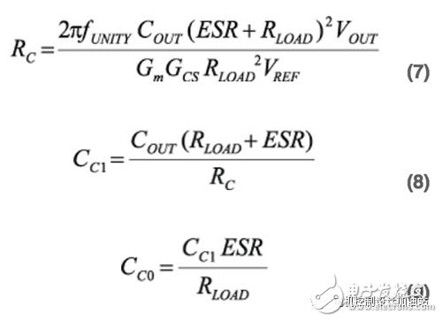
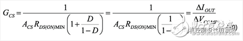
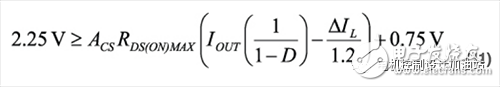
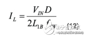
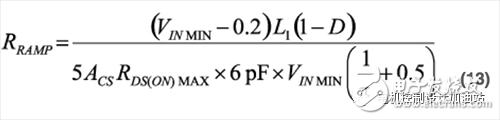
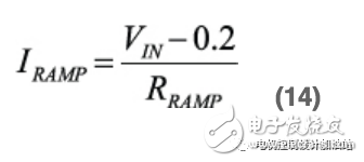
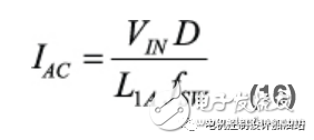
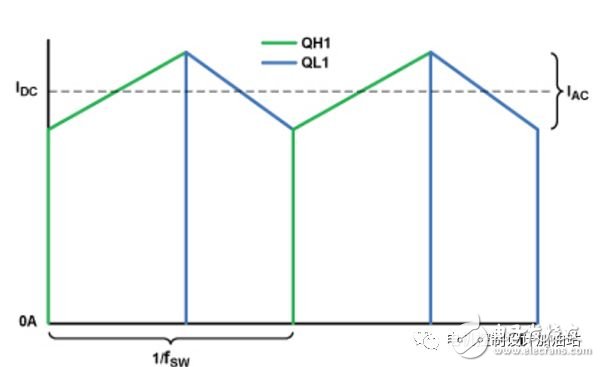
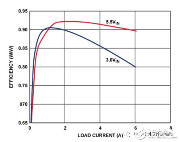
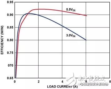
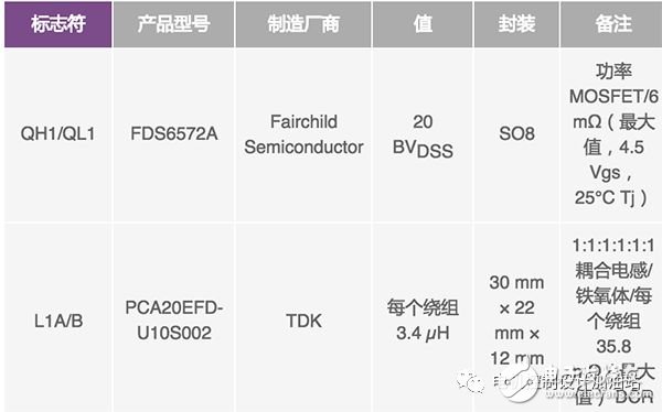
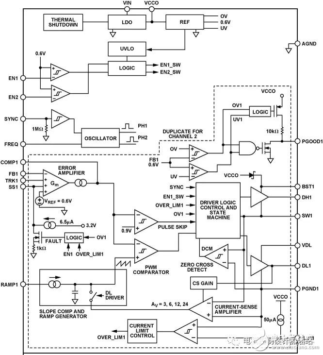
Demand for high-efficiency, in-phase DC-DC converters is growing in many markets, and these converters can operate in buck or boost mode, which reduces or increases the input voltage to the required regulated voltage with the lowest cost. And the minimum number of components. The inverting SEPIC (Single-Ended Primary Inductor Converter), also known as the Zeta Converter, has many features that support this feature (Figure 1). The working principle and the implementation of the dual-channel synchronous switch controller ADP1877 can be analyzed to understand its useful characteristics in this application. Figure 1. Inverting SEPIC topology The primary switch QH1 and the secondary switch QL1 operate in reverse. During the on-time, QH1 turns on and QL1 turns off. Current flows along two paths, as shown in Figure 2. The first path is from the input through the primary switch, energy transfer capacitor (CBLK2), output inductor (L1B) and load, and finally flows back to the input through the ground. The second path is from the input through the primary switch, ground reference inductance (L1A) and ground return to the input. Figure 2. Current flow diagram; QH1 is closed and QL1 is open. During the off period, the switch position is just the opposite. QL1 is turned on and QH1 is turned off. The input capacitor (CIN) is open, but current continues to flow through the inductor along two paths, as shown in Figure 3. The first path is from the output inductor through the load, ground and secondary switches back to the output inductor. The second path is from the ground reference inductor through the energy transfer capacitor, and the secondary switch flows back to the ground reference inductor. Figure 3. Energy transfer diagram; QL1 is closed and QH1 is open. Using the principle of the volt-second balance of the inductor and the principle of the charge-charge balance, the balanced DC conversion ratio specified in Equation 1 can be obtained, where D is the duty cycle of the converter (the on-time portion of one cycle). The above equation shows that if the duty cycle is greater than 0.5, the output will obtain a higher regulated voltage (boost); if the duty cycle is less than 0.5, the regulated voltage will be lower (buck). In addition, other related results can be analyzed: in a lossless system, the steady-state voltage on the energy transfer capacitor (CBLK2) is equal to VOUT; the DC current flowing through the output inductor (L1B) is equal to IOUT; the ground reference inductance (L1A) flows through The DC current value is equal to IOUT &TImes;VOUT/VIN. The energy transfer capacitor also provides DC to VOUT isolation. This feature is useful when there is a risk of output shorts. The analysis also shows that the output current in the inverting SEPIC is continuous, resulting in a lower peak-to-peak output voltage ripple for a given output capacitor impedance. This allows the use of smaller, less expensive output capacitors; in contrast, in a discontinuous output current topology, large and expensive capacitors are required to achieve the same ripple requirements. Typically, the secondary switch (QL1) is a unidirectional power diode that limits the peak efficiency of this topology. However, using a channel from Analog Devices' dual-channel synchronous switching controller ADP1877 (see Appendix) and using a bidirectional MOSFET as a secondary switch, a "fully synchronized configuration" inverted SEPIC can be designed. In this way, the peak efficiency will be greatly improved, while reducing the size and cost of the converter with an output current greater than 1 A. Figure 4 shows the power stage of a fully synchronous inverting SEPIC configuration. It is implemented in the ADP1877 and requires only three small, inexpensive additional devices (CBLK1, DDRV, and RDRV) with negligible power consumption. Figure 4. Synchronous inverting SEPIC power stage, using channel 1 of the ADP1877 The ideal steady-state waveform of the inverted SEPIC is shown in Figure 5. Channel 1 Switch Node SW1 (see Appendix Figure A) switches between VIN + VOUT (on-time) and 0 V (off-time). Connect the charge pump capacitor CBST to SW1 to apply a voltage of approximately VIN + VOUT + 5 V to the bootstrap upper rail (BST1 pin) of the high-side internal driver and the output of the high-side driver during the on-time (DH1) Foot), thereby enhancing the primary floating N-channel MOSFET switch QH1. The clamp diode DDRV ensures that the voltage on CBLK1 during steady-state output is approximately VOUT + VFWD (DDRV), which is referenced to the voltage at the DH1 pin of the ADP1877 to the QH1 gate. During the off time, when the X node voltage is approximately –VOUT, the voltage on CBLK1 prevents the primary switch from generating a gate-to-source voltage above its threshold. Figure 5. Ideal waveform for synchronous inverted SEPIC (ignoring dead band) The ADP1877 has a pulse skip mode that, when enabled, reduces the switching rate and provides only enough energy to keep the output voltage stable at the output, improving efficiency at small loads and greatly reducing gate charge and switching losses. This mode is enabled in both synchronous inverting SEPIC and synchronous buck topologies. The DC-DC converter circuit shown in Figure 4 requires only one channel of the dual-channel ADP1877, so the other channel can be used in either topology. Inductive coupling and energy transfer capacitor In Figure 4, power inductors L1A and L1B are shown coupled to each other. In this topology, the purpose of the coupled inductor is to reduce the ripple of the output voltage and inductor current and to increase the maximum possible closed-loop bandwidth, as explained in the next section. Although these inductances are coupled to each other, it is not desirable that the coupling be too tight so that a large amount of energy of one winding is transmitted through the core to the other winding. To avoid this, the leakage inductance (LLKG) of the coupled inductor must be determined and the appropriate energy transfer capacitor (CBLK2) selected so that the magnitude of its complex impedance is the complex series impedance of the leakage inductance and the individual winding resistance (DCR). 1/10, as shown in Equations 2, 3, and 4. Designing the circuit in accordance with this relationship minimizes the energy transmitted by the coupled core. The leakage inductance can be calculated from the coupling factor provided in the coupled inductor data sheet. The turns ratio is preferably 1:1 because for a given level of output voltage ripple, each winding requires only half of the inductance required for the discrete inductor. You can use a turns ratio other than 1:1, but the results will not be accurately described by the equations in this article. Small signal analysis and loop compensation Complete small-signal analysis of the inverting SEPIC converter is beyond the scope of this article, but a complete analysis would be more academic if the following principles are followed. First, many complex impedance interactions at the resonant frequency (fRES) must be calculated in order to find the upper bound of the target crossover frequency. When the inductor is decoupled, this frequency is reduced, resulting in a significant reduction in the maximum possible closed loop bandwidth. At this frequency, there may be a "high Q" phase hysteresis of 300° or greater. In order to avoid the problem that the converter has a small phase margin over the entire load range, the target crossover frequency (fUNITY) should be 1/10 of fRES. The damping of this resonance is mainly determined by the output load resistance and the DC resistance of the coupled inductor. To a lesser extent, the damping also depends on the equivalent series resistance (ESR) of the energy transfer capacitor and the on-resistance of the power MOSFETs (QH1 and QL1). Therefore, it is not surprising that the characteristics of the closed-loop transfer function change significantly at this frequency as the output load resistance changes. The coupling coefficient is usually not a parameter that can be precisely controlled, so the target crossover frequency should be set to a value 10 times lower than fRES (assuming fRES is less than the switching frequency fSW). When the fUNITY setting is appropriate, the standard "Type II" compensation can be used - two poles and one zero. Figure 6 shows the equivalent circuit of the ADP1877 feedback loop in a synchronous inverted SEPIC buck/boost topology. The upper frame contains the power stage and current loop, and the lower frame contains the voltage feedback loop and compensation circuit. Figure 6. Power stage and compensation scheme for the ADP1877 with internal current sense I-loop in a synchronous inverting SEPIC topology The compensation component value in the lower frame can be calculated by: The transconductance GCS of the converter is calculated using the following equation: COUT is the output capacitance of the converter. ESR is the equivalent series resistance of the output capacitor. RLOAD is the minimum output load resistance. The ACS is the current sense gain and for the ADP1877 it can be selected in discrete steps from 3 V/V to 24 V/V. Gm is the transconductance of the error amplifier, which is 550 μs for the ADP1877. VREF is the reference voltage connected to the positive input of the error amplifier, which is 0.6 V for the ADP1877. GCS is a frequency-independent gain term that varies with the enhanced secondary switching resistance RDS(ON). The highest crossover frequency is expected to occur when this resistance and duty cycle D are lowest. To ensure that the compensation clamp voltage is not reached at the maximum output current, the highest value of the selected current sense gain (ACS) should meet the following conditions: Where ∆IL is the peak-to-peak inductor ripple current. If the slope compensation is excessive, the accuracy of the equation here will decrease: the DC gain will decrease and the output filter will cause the frequency position of the main pole to increase. Slope compensation For the synchronous inverting SEPIC implemented with the ADP1877, the subharmonic oscillation in the current mode controller 2 must be considered. By setting RRAMP as follows, you can set the quality factor of the sampling pole to 1, thus preventing subharmonic oscillations 3 (assuming the fUNITY setting is appropriate). It is worth noting that as the enhanced secondary switching resistance RDS(ON) decreases, the Q of the sampling pole also decreases. If this factor, together with other related tolerances, causes Q to be less than 0.25, then a simulation should be performed to ensure that the converter does not have excessive slope compensation, and is not too biased toward voltage mode, given the tolerances. The value of RRAMP must be such that the current on the ADP1877 RAMP pin is in the range of 6 μA to 200 μA. Equation 14 is as follows: Power device stress It can be seen from the current flow diagrams in Figures 2 and 3 that the power MOSFET is to carry the sum of the inductor currents after being turned on. Therefore, the DC component of the current flowing through the two switches is: If the coupling ratio of the inductor is 1:1, the current AC component flowing through the two switches is: Knowing these values, you can quickly calculate the rms current through each switch. These values ​​together with the RDS(ON)MAX of the selected MOSFET ensure thermal stability of the MOSFET while low power consumption to meet efficiency requirements. Figure 7. Ideal Current Waveform for Synchronous Inverting SEPIC (Ignore Dead Band) Accurately calculating the switching loss of the primary switch is beyond the scope of this article, but it should be noted that when changing from a high-impedance state to a low-impedance state, the voltage swing on the MOSFET is approximately VIN + VOUT to 0V, and the current swing through the switch is 0 A to IOUT[1/(1–D)]. Since the swing is so high, switching losses can be the main loss, which is a point to note when choosing a MOSFET; for MOSFETs, the reverse transfer capacitor (CRSS) is inversely proportional to RDS(ON). The drain-to-source breakdown voltage (BVDSS) of the primary and secondary switches must be greater than the sum of the input voltage and the output voltage (see Figure 5). The peak-to-peak output voltage ripple (∆VRIPPLE) can be approximated by: The current rms value (I rms COUT) flowing through the output capacitor is: The peak-to-peak inductor current (∆IL) represented by Equation 12 depends on the input voltage, so it must be ensured that when this parameter is changed, the output voltage ripple does not exceed the specified value, and the rms current flowing through the output capacitor does not exceed Its rating. For synchronous reverse SEPIC implemented with the ADP1877, the sum of the input voltage and the output voltage must not exceed 14.5 V because the charge pump capacitor is connected to the switch node and its voltage reaches VIN + VOUT when the primary switch is turned "on". Laboratory results Figure 8 shows the efficiency of the synchronous reverse SEPIC versus load current for 5 V, 3 V, and 5.5 V inputs. This is common for applications that need to switch between 3.3 V and 5.0 V input rails, or when adjusting the input voltage in real time to optimize system efficiency. With a 1 A to 2 A load, the converter's efficiency exceeds 90% regardless of the input voltage above or below the output voltage. Figure 8. Efficiency versus load current The list of power device materials associated with Figure 8 is shown in Table 1, using only common off-the-shelf devices. A comparable asynchronous design uses an industry-leading Schottky diode with a low forward voltage drop instead of QL1, which is nearly 10% less efficient at full load at both input voltages. In addition, asynchronous designs are larger, more expensive, and may require expensive heat sinks. Table 1. Power Devices Conclusion Many markets are increasingly demanding high efficiency non-inverting converters with output voltages above or below the input voltage (boost/buck). ADI's dual-channel synchronous switching controller, the ADP1877, allows low-loss MOSFETs to replace high-loss power diodes commonly used in power stages, increasing efficiency, reducing cost, and reducing circuit size, resulting in demanding energy requirements. As long as a few principles are followed, the component values ​​required for reliable compensation can be quickly calculated and high efficiency can be achieved with common off-the-shelf devices. Reference circuit Barrow, Jeff. "Reducing Ground Bounce in DC-to-DC Converters—Some Grounding EssenTIals." Analog Dialogue. 41-2, pp. 2-7. 2007. 1Ćuk, Slobodan and RD Middlebrook. "Coupled-Inductor and Other Extensions of a New OpTImum Topology Switching DC-DC Converter." Advances in Switched-Mode Power Conversion. Volumes I & II. Irvine, CA: TESLAco. 1983. 2Erickson, Robert and Dragan Maksimović. Fundamentals of Power Electronics. Chapter 12, SecTIon 1. Norwell, MA: Kluwer Academic Publishers. 2001. 3Ridley, Raymond. "A New Small-Signal Model for Current-Mode Control." PhD Dissertation, Virginia Polytechnic Institute and State University. November 1990. appendix The ADP1877 is a Flex-ModeTM (ADI's proprietary architecture) dual-channel switching controller, shown in Figure A, with an integrated driver that drives an N-channel synchronous power MOSFET. The two PWM outputs are phase shifted by 180° to reduce the input rms current, thus minimizing the required input capacitance. Figure A. Schematic block diagram of the ADP1877. Only channel 1 is shown; channel 2 is identical, with a suffix of 2. The ADP1877 has a built-in boost diode, which reduces overall component count and system cost. At low loads, it can be set to a high efficiency pulse skip mode of operation or a PWM continuous conduction mode of operation. The ADP1877 has an externally adjustable soft start function, output overvoltage protection, external adjustable current limit, power good indication, and a programmable oscillator frequency from 200 kHz to 1.5 MHz. The output voltage accuracy is ±0.85% over the operating temperature range of –40°C to +85°C and ±1.5% over the junction temperature range of –40°C to +125°C. It operates from a 2.75 V to 14.5 V supply and is available in a 32-pin, 5 mm × 5 mm LFCSP package. Author: Matt Kessler Matt Kessler is an applications engineer for Power Management Products in the Customer Applications Group in Fort Collins, CO. Responsible for technical support for a wide range of a products and customers, Matt is also one of the original architects and developers of ADIsimPower. Matt earned His BSEE from the University of Texas at Dallas and is currently pursuing his MSEE at Colorado State University. He has been with Analog Devices since 2007.