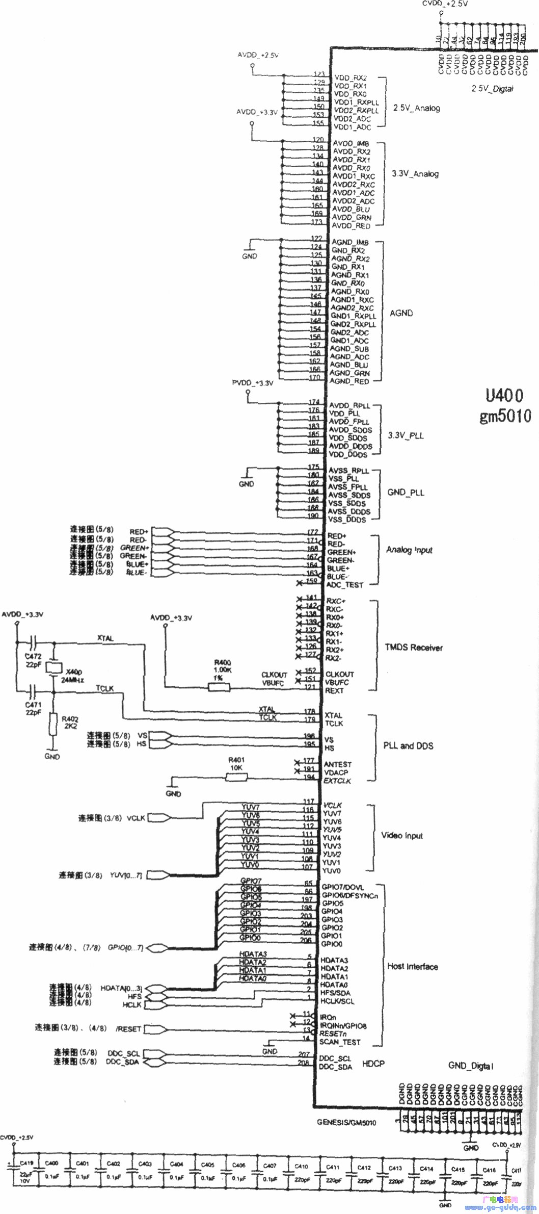
The Gm5010 is a high-performance 208-pin microchip developed by Genesis, primarily designed for liquid crystal display (LCD) processing. It integrates a powerful flat panel image processor, multiple signal input channels, an OSD control circuit, an X86 microprocessor, a PLL clock generator, and intelligent ADC image processing modules. This makes it ideal for advanced display applications. Gm5010 Image Digital Processing Control Circuit (a) Gm5010 Image Digital Processing Control Circuit (b) Pin 1 (HCLK/SCL): Line clock signal input or serial clock signal input. Pin 2 (HFS/SDA): Line pulse signal input or serial data signal input. Pins 3, 29, 45, 57, 70, 87, 101, 201, 9, 21, 31, 43, 61, 73, 83, 95, 113, 118, 192, 199: Ground for digital circuits. Pins 4, 30, 46, 58, 72, 88, 102, 202: Power supply for digital circuits at 3.3V. Pins 5, 6, 7, 8: Digital signal input, sourced from pins 23, 4, 5, and 6 of U501 (M6759). Pins 10, 22, 44, 32, 62, 74, 84, 96, 114, 119, 193, 200: Power supply for digital circuits at 2.5V. Pins 11, 12: Unused. Pin 13 (RESETn): Reset terminal, controlled via SW500 and powered by pin 2 of U503. Pin 14 (SCAN_TEST): Test pin, connected to ground. Pins 15–28: Bootstrap simulation line input for bootstrapping operations. Pins 33–40: Display port for outputting 8-bit blue primary DA signal. Pins 41–52: Display port for outputting 8-bit green primary DA signal. Pins 53–64: Display port for outputting 8-bit red primary DA signal. Pin 67 (DHS): Output line scan signal. Pin 68 (DVS): Output field scan signal. Pin 69 (DEN): Output DEN signal. Pin 71 (DCLK): Output clock signal. Pins 75–82: Display port for outputting 8-bit blue primary DB signal. Pins 85–94: Display port for outputting 8-bit green primary DB signal. Pins 97–106: Display port for outputting 8-bit red primary DB signal. Pins 107–116: Video signal input port for 8-bit YUV signal, sourced from U800 (SAA7114H). Pin 117 (VCLK): Clock signal input. Pins 163, 164, 167, 168, 171, 172: Input for R, G, B forward and reverse image signals. Pin 178 (XTAL): Clock oscillation input, using an external 24MHz voltage-controlled crystal oscillator. Pin 179 (TCLK): Clock oscillation output, using an external 24MHz voltage-controlled crystal oscillator. Pin 195 (HS): Line sync signal input. Pin 196 (VS): Field sync signal input. Pins 206, 205, 204, 203, 198, 197, 66, 65: Input for 8-bit GPIO signal. Pin 207 (DDC_SCL): I2C bus clock line, connected to VGA socket and U203 (24LC21A) memory. Pin 208 (DDC_SDA): I2C bus data line, connected to VGA socket and U203 (24LC21A) memory. Pins 123, 129, 135, 149, 150, 153, 155: 2.5V power supply lines. Pins 120, 128, 134, 140, 143, 144, 160, 161, 165, 169, 173: 3.3V power supply lines. Pins 174, 176, 181, 183, 185, 187, 189: 3.3V power supply lines. Overhead Line Fittings,Nylon Spindle For Insulator,11kv Spindle For Insulator,Hot Dipped Galvanized Spindle For Insulator Shahe Yipeng Import and Export trading Co., LTD , https://www.yppolelinehardware.com