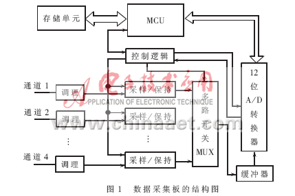
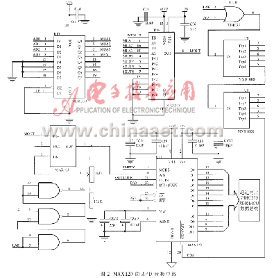
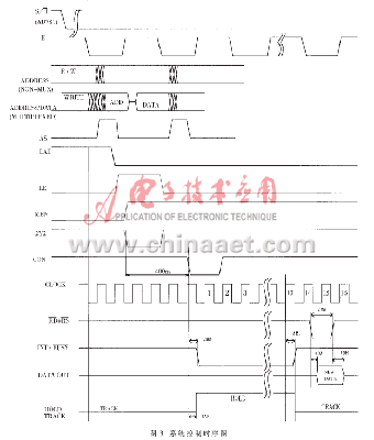
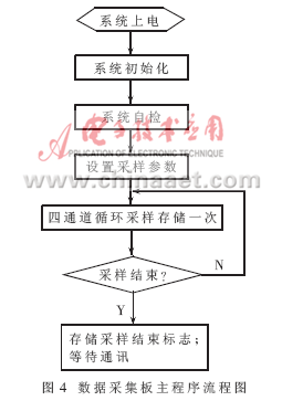
In the passive safety study of automobiles, the collision experiment is a key experiment, and the experimental data of the whole vehicle or parts and model dummy can be obtained by appropriate measurement technology to ensure the success of the experiment. There are two main types of electrical measurement technology in automobile crash experiments: one is the long-distance line measurement method; the other is the vehicle data acquisition. With the deepening of research and the improvement of measurement technology requirements, the need for the latter measurement method is more urgent. This article refers to the address: http:// As a high-speed and large-impact experiment, the vehicle crash test needs to be able to withstand large shocks, many channels, reliable storage of large-capacity data, and accurate triggering. The crash test vehicle test system in foreign countries has formed a relatively mature product, but the price is quite expensive. Domestic test equipment is also developed in their respective fields and is not suitable for use in harsh environmental conditions of collision experiments. The data acquisition board is the core of this in-vehicle test equipment. This paper has deeply studied a data acquisition board used in the on-board equipment. According to the design rules of the frontal collision occupant protection design (CMVDR294), the sampling frequency of each channel of the data acquisition board in the in-vehicle test system is designed to be 10 kHz, and the analog signal is converted into a digital quantity using a 12-bit digital length. Taking into account the need for subsequent analysis and processing of the signal, the signal acquisition of each channel is completely synchronized in the system design. 1 Design principle of data acquisition board The vehicle test system uses multiple data acquisition boards to work in parallel, and the single master module is responsible for triggering the judgment. Each data acquisition board acts as a separate sub-module in the entire test system, using a separate MCU to complete the control of the acquisition board. Most of the similar acquisition boards use an A/D chip to collect the signal of one channel to meet the requirements of simultaneity. However, it is difficult to expand a large number of channels, and the whole system is very complicated, which reduces the reliability during collision. In this board design, each data acquisition board uses an A/D chip to achieve simultaneous acquisition of four channel signals. This improves the reliability of the acquisition board by reducing the number of chips. The structure of the acquisition board is shown in Figure 1. When the test system is working, the data acquisition board continuously converts the sensor signals into digital quantities, which are cyclically stored in the memory of the data acquisition board. When the data acquisition board receives the collision end signal generated by the control module, it will generate an interrupt, stop data acquisition, and wait for communication with the ground microcomputer. 2 hardware components 2.1 MCU and address space The MCU of the data acquisition board adopts MOTOROLA's high-end 8-bit single-chip MC68HC-711E9[3]. This kind of single-chip microcomputer has a wide range of applications under the complicated working conditions of automobiles, and has also been applied in a safety airbag controller. Practice has proved that its impact resistance meets the requirements of this data acquisition board. It has 8 data lines and 16 address lines in extended mode, which can address 64KB of space. The MCU addresses the data memory and the program memory in a unified manner. In this 64KB space, the RAM area and the register area of ​​the microcontroller are rearranged by setting the relevant registers, so that $0000~$CFFF in the configured address space. It is a continuous data memory area. However, due to the maximum address of 64KB of the microcontroller, the space of the data memory is small. Since each data acquisition board stores four channels of analog conversion results, the data memory must have a large enough capacity to store signals for a longer period of time. Two 512 KB SRAM chips 628512 are used for this purpose as an external data memory. The MCU has only 16 address lines, so the page-expanded memory technology is used, and the output port lines of the four PORT A are used to form eight 64 KB pages per 628512. $0000~$CFFF can be used to store data on each page. Therefore, the available data storage space of the system is 16×52=832 KB, that is, the data storage capacity of each channel is 208 KB. If the sampling rate is calculated at 10 kHz, and each conversion result is 12 bits, which occupies a maximum of 2 bytes of space, the data time of each channel that the system can save is 208 ÷ (10 × 2) = 10.4 s, which satisfies the system requirements. 2.2 Signal Conditioning Circuit EG&G's piezoresistive sensor is used in the car crash test. It integrates a voltage regulator device and has a temperature compensation function. It has its own amplifier, which makes the output range of the sensor become ±2V. The signal conditioning circuit firstly amplifies the signal of the sensor by 2 times, so that the signal output range of the sensor can be matched with the general A/D analog input range of ±5V, which improves the conversion accuracy of the system. The amplifying circuit part adopts the AD620 instrument amplification chip AD620, and the hardware can make the magnification adjustment between the gear positions 1, 2, 5, 10, so that the signal conversion can be resolved in experiments with different impact strengths. The rate is higher. The amplified signal is also filtered by the programmable filter composed of MAX291 and sent to the A/D conversion circuit. The filter frequency is set to 2 kHz as required by the collision regulations. 2.3 A / D conversion circuit The A/D converter is the core of the data acquisition board. This board design selects MAXIM's 12-bit high-speed A/D conversion chip MAX120[2], which has a bipolar ±5V voltage input range to complete a conversion. The time is 1.6 microseconds with an internal sample-and-hold circuit and a low drift voltage reference with a standard microprocessor (μP) interface. An A/D conversion circuit composed of such a chip is shown in FIG. 2. The MAX308 [2] in Figure 2 is a MAXIM multiplexer with low on-resistance (less than 100 Ω) and low leakage current. The typical switching speed is 85 nanowires. The input impedance of the MAX120 is 6kΩ. If the A/D chip is directly connected to the multiplexer, the voltage division of the input signal on the multiplexer will cause an error that is close to the required accuracy range. For this reason, A// An input buffer is added in front of the D chip. MAXIM's high-speed buffer amplifier MAX405[2] is used here. Its input impedance is 2.5MΩ and the output impedance is 0.01Ω. Therefore, the voltage drop error caused by the signal on the multiplexer is only the buffer itself is close to zero internal resistance. It ensures that the signal will not cause large distortion at the input to the A/D chip. This method is greatly improved in the actual design. Since only one A/D chip is used in the data acquisition board, in order to ensure that the conversion of each signal is synchronized, a sample-and-hold circuit (AD781) is added to each signal before the multi-way switch in the design [1]. When the acquisition board is working, in each sampling cycle, the sampling/holding signal is first sent so that the signals of each channel are simultaneously sampled and then enter the holding state, and then the multiplexer gradually strobes each analog signal into the A/D converter. The acquisition circuit uses the MAX120's full control mode (Mode 1). The system operation sequence formed in this way is shown in Figure 3. When the system is working, the switching channel and the startup A/D converter use the same instruction: STAA $DFF0,CHANEEL When this instruction is executed, the logical combination of the LAE and E clock signals formed by the decoding makes LE a high level, strobing 74HC373, the channel number CHANGEEL on the data bus (corresponding to AD2, AD1, AD0 of the data bus) and more. The switch control signal MEN appears on the address selection terminal and the control terminal of the MAX308 through the 74HC373, and the analog signal of the corresponding channel is output to the buffer MAX405 through the MAX308. On the next E clock, LE goes low, the 74HC373 latches the channel number and the control signal MEN, and the analog signal of the selected channel is always held at the MAX308 output until the next channel select command is executed. While the MAX308 is strobed, the LAE signal is also logically combined with the write signal 2Y2 as the enable signal for the A/D converter MAX120. Considering that the analog signal of the selected channel appears at the output of the MAX308 requires a certain settling time to achieve the proper accuracy, while the MAX120 operating in mode 1 also requires a certain sampling time (350 nanoseconds) to capture the input. The analog signal, therefore, requires a certain time interval between the channel switching of the MAX308 and the start of the MAX120 to ensure the accuracy of the conversion result. For this design, the LAE is matched with the 2Y2 signal, and then the two MXD1000 delay chips are delayed by 400 nanoseconds as the start signal CON of the A/D converter. After the conversion is started, the MCU judges that the conversion is completed by the signal connected to the PA0 pin. At the same time as the execution of the read data instruction, the conversion result is controlled by the read signal 2Y3, sent to the data bus of the MCU through the bus buffer 74HC245, read into the MCU, and then written to the memory cell. 2.4 storage unit The data storage unit in the design selects two RAM chips 628512. Considering that the actual experiment is a high-intensity impact, it is replaced with a non-volatile SRAM. The HK1255 is a non-volatile SRAM chip that is fully compatible with 628512. It can be used directly in place of the 628512, and its built-in lithium battery can save data for a long time without external power supply. This ensures that even if the large impact strength is encountered in the experiment, the system power supply is broken, the data collected in the experiment can be saved, which greatly enhances the reliability of the system. 3 acquisition board software design The data acquisition board software mainly implements two functions: completing the sampling and storage of the analog quantity; and communicating with the PC online. The main program flow is shown in Figure 4. After setting the sampling parameters, the data acquisition board performs a cyclic sampling on the four analog signals. After the storage is finished, it is determined according to the sampling end flag whether the data collection has been completed. The sampling end flag is set when the interrupt subroutine is executed when the main module determines the trigger and the external interrupt (IRQ) response in the data acquisition board. During the acquisition process, the program continuously stores the collected data. When the set address pointer reaches the bottom of the data storage area, it is set to redirect to the top of the storage area, and the original data is refreshed with the re-stored data. After the end of sampling, successive $0F $FFs are stored after the last sampled data in the data memory area as a flag for the end of sampling. After the data is transmitted to the ground PC, in the data processing, the collected collision waveforms of the respective channels can be determined and selected according to the continuous $0F $FF flag. This cyclic storage mode preserves the waveforms before and after the required collision time for the maximum length in a limited storage space. The function of the online communication software is to set the sampling parameters before the experiment, and transfer the data in each data acquisition board memory to the ground PC after the experiment. This paper introduces the data acquisition board developed by the self-developed vehicle test equipment for automobile crash test. The data acquisition board has the following characteristics: 1 The acquisition board is controlled by a separate MCU, and the test system does not require the intervention of the ground microcomputer during the experiment; 2 realizes four-channel synchronous high-speed data acquisition with one A/D chip, and analyzes the text. The working sequence; 3 realizes the reliable storage of large-capacity data in the collision experiment under the big impact environment; 4 The design uses the idea of ​​circular storage to make maximum use of the storage space; 5 can form more channels together with other modules Number of acquisition systems. No adjustable components were used in the overall board design, and good curing and buffering were applied to the system. These measures also greatly improved the impact resistance and reliability of the system. In the comparison experiment with the original measurement system, for the same input signal, the on-board test system using the data acquisition board and the original system have a high consistency, and the full-scale error is less than 0.8%, in accordance with the system. The accuracy requirements have achieved good results. At the same time, this data acquisition board can also be used in other test experiments that require high-speed synchronous acquisition.
It adopts high-quality battery monomers grouped and screened and designed by special mechanical structure to assemble all ranges of built-in BMS batteries.
Voltage levels: 12V, 24V, 36V, 48V, 96V, 110V, 220V, 330V, 380V, 440V, 600V.
Rated battery volumes: 10 ~ 2000Ah.
Battery types: lithium iron phosphate (LiFePO4), Valve Regulated Lead Acid (VRLA), high rate Nickel Cadmium Battery, nickel-hydrogen power, silver zinc battery and so on.
Main functions of BMS: capacity forecast, over current, over voltage, over charge, over discharge, over-temperature protection, single voltage balance, abnormal alarm, CAN-BUS communication, programmable parameters.
Bms For Lithium Ion Battery,Li Ion Battery Management System,Lithium Battery Management System,Li Ion Bms Xinxiang Taihang Jiaxin Electric Tech Co., Ltd , https://www.chargers.be