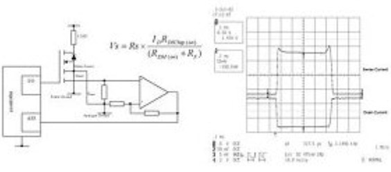
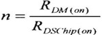
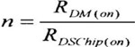
Engineers may encounter challenges in designing any power application when designing a power system for automotive electronics . Because the power device MOSFET must be able to withstand the most demanding environmental conditions. Ambient operating temperatures above 120 °C can increase the junction temperature of the device, causing reliability and other problems. In extreme environments (such as automotive electronics applications under the hood), a rapid rise in temperature can cause the MOSFET to turn on unexpectedly, causing the threshold voltage to approach zero volts. This article refers to the address: http:// In addition, the MOSFET must be able to withstand high voltage spikes caused by switching off transients and load dump faults. A large number of connectors in the electrical wiring (located in place to facilitate assembly and repair wiring) also greatly increase the likelihood of electrical connection to the device being interrupted. The automotive industry is very concerned about quality and reliability, so MOSFETs must comply with the internationally recognized AEC Q101 standard. Every aspect of the above is very important. But there is another challenge, which is to provide higher energy efficiency. In the past few years, the proportion of electronically controlled car functions has increased dramatically. Therefore, the number of semiconductors in the car is also increasing. Some vehicles have more than 100 ICs. MOSFETs must be able to meet the ever-increasing energy requirements of powering more ICs. The development of the automotive subsystem itself also requires more energy. Electric steering systems and anti-lock braking systems, which are increasingly popular in light vehicles, are two good examples. In summary, all of these trends have spurred a strong demand for ICs that can carry larger currents. In order to meet the demand for higher current, semiconductor companies must develop power MOSFETs that can reduce the on-resistance (resistance value when current flows). MOSFETs fabricated using Trench semiconductor fabrication processes help reduce on-resistance values ​​by 20% to 40% compared to conventional MOSFETs. But in recent years, advances in power MOSFET technology have reduced the on-resistance per unit silicon area to extremely low levels, so device manufacturers must now look for other ways to improve their products. This is especially important when manufacturing devices with low drain-to-source voltages using high density trench technology. Protection is one of the strategies that IC companies use to provide performance benefits to their automotive customers. More MOSFET options Today, automotive designers who choose MOSFET devices have only two options: 1. Choose a “simplified†PowerMOS with no protection strategy; 2. Choose a fully protected device that automatically shuts down when environmental conditions are out of specification. Unfortunately, a fully protected device with additional logic and protection circuitry has the disadvantage that the cost of implementing protection is too high. Therefore, leading IC companies are already developing a new type of device to combine the advantages of both. Philips Semiconductors' TrenchPLUS product line is a good example. TrenchPLUS fully integrates TrenchMOS technology and additional functionality into the chip. The TrenchMOS process, introduced in 1996, reduced the on-resistance RDS(on) of the power MOSFET by half. The combination of TrenchMOS and other features provides the ability to protect the system, save space, and eliminate the need for expensive smart power devices. TrenchPLUS technology The TrenchPLUS device integrates on-board temperature and current sensing features with additional resistors and diodes (including ESD protection). The TrenchPLUS solution helps system engineers create designs that measure system activity during work to improve safety and optimize performance. Figure 1 shows a typical component set for a TrenchPLUS type device. Figure 1: Additional features that the TrenchPLUS device may have The highlighted components form a feature board that integrates the functions into the MOSFET. These components are clockwise from the upper right corner: temperature sensing diodes, current sensors, clamping diodes (internal diodes, not shown), and gate resistors. The voltage-sensitive gate oxide is protected from hazardous electric fields by the well-known protection features of clamping diodes and gate resistors. To protect the device from excessive temperatures, Philips integrates temperature-sensing diodes on the surface of the chip. The reason for this integration is that only direct measurement of the junction temperature ensures timely detection of dangerously high gate temperatures. To accurately measure current, a current sensor can be integrated into a field effect transistor (FET). This eliminates the need for low impedance shunt resistors. Temperature sensing A conventional solution for directly measuring chip temperature is to add a comparator and several passive components. However, as the design became more sophisticated, better solutions emerged. TrenchPLUS replaces comparators and passive components with microcontrollers. Since accuracy is critical to the temperature measurement of the MOSFET, we will illustrate this solution from this perspective. In theory, the accuracy of a temperature sensor depends on three factors: 1. The error of the forward voltage Vf; 3. Selection of reference voltage Vfref. Figure 2 shows the effects of these three factors more clearly. Figure 2: Ttrip changes with Vf, Sf It can be observed from the figure that the intrinsic variation of Vf adds a fixed offset to the Ttrip. The change in Sf is represented by the change in slope. Too small a temperature coefficient can cause the device to still operate when the temperature exceeds its maximum operating temperature, thereby damaging the life of the device. Conversely, a temperature coefficient that is too high will result in an unpleasant false turn-off at temperatures below the Ttrip. Both of these factors have an impact on the protection strategy adopted. In order to calculate the total error, the errors of Vf and Sf should be summed. Please note that if the room temperature value of Vf. is measured, the accuracy of the device will double. The error of Vf can be eliminated by adjusting Vfref so that only the error associated with the slope remains. The most accurate technique that can be used to achieve this is to get the characteristics of each device, but this is not realistic for most product lines. Current sensing A realistic method of measuring the internal current of a MOSFET without using a precision power resistor of less than 1 ohm is current sensing. Even shunt resistors below 1 ohm can generate a large amount of heat loss, affecting energy efficiency and thermal balance throughout the system. In current sensing, a small portion of the MOSFET cell is used for current measurement. Since all the cells in the device are identical and the leakage current is evenly distributed between these cells, the total leakage current can be calculated by measuring the current of a small number of cells and multiplying by a known scaling factor. Philips' 7-pin D2PAK is used to connect the temperature sensing element to the current sensing element. The ratio of current flowing from the main FET device to the inductive FET device is referred to as the "induction ratio" (indicated by n). This parameter is defined by keeping the measurement terminal and the source terminal at the same voltage. For example, in Philips' TrenchPLUS devices, this ratio is nominally 550. This ratio can be changed to meet the specific requirements of the customer. In order to achieve the highest accuracy, including some designers, the virtual grounding method is used instead of the inductive resistance method. However, for automotive applications, the inductive resistance method provides a lower cost solution and is therefore more suitable for automotive applications. Inductive resistance method As described above, the sense resistor Rs can be connected between the sense output and the Kelvin source to accurately measure the current. This method provides a simple current to voltage conversion and the conversion value can be read directly from the microcontroller's analog input. The voltage on the sense resistor cannot be greater than the voltage on the master device, however, an op amp may be required to amplify the signal to a more suitable level. This configuration is shown in Figure 3. Figure 3: Inductive Resistor Current Measurement Circuit This circuit does not require a negative supply as long as the common mode range of the op amp includes ground. The geometric induction ratio n is: Where RDM(on) is the on-resistance of the sense FET, which is equal to the on-resistance of the main FET minus the source lead resistance. The additional sense resistor increases the effective sense ratio, so the value becomes n' and the formula is: It is worth noting that the sensing signal contains the peak error of the switch. The cause of these false peaks is the difference in the ratio of currents in the linear and fully enhanced working area, and is related to the circuit. Equation 2 shows that there are two major sources of error in this circuit: 1. inherent error in the manufacturing process; 2. Depends on the temperature of the main FET and the sense FET. Between 25 ° C and 150 ° C, the on-resistance of the power MOSFET is approximately doubled when it is turned on. On the other hand, the sense resistor is independent of temperature. Therefore, it can be seen that when using this method, 1. the sensing ratio is related to temperature; 2. The error is greater than the error using the virtual ground circuit. Package method When talking about MOSFETs, you can't talk about the package, which is especially important for automotive applications. Although D2PAK is the original package with TrenchPLUS devices, it now has a smaller, more thermally efficient package. Philips' SOT669 LFPAK offers higher heat dissipation from the SO8's compact package footprint. Its internal structure overcomes the limitations of SO8. Its thermal resistance can be compared to a larger package, which helps maintain the lowest possible operating temperature. The LFPAK is very compact – it is only 1.1mm thick and 40% thinner than the SO8. This innovative internal structure makes its inductance much lower than other packages. The 40V HPA LFPAK package offers the advantages of the compact size of the SO8 and the superior thermal performance of larger packages such as DPAK. In a conventional power package, the main heat dissipation path is perpendicular to the assembly point and into the PCB. However, LFPAK also conducts a large amount of heat up and out through the source wires, making its thermal resistance much lower than SO8, even compared to much larger packages such as DPAK and D2PAK. Summary of this article Automotive electronics design engineers have many benefits in using additional sensors in their powerMOS designs. By capturing information about the chip's local temperature/current, designers can save space and reduce system cost. And to achieve this goal, while advancing the scope of the design. A trade-off between cost and performance is often required, and this consideration is not required for this device. This device fills the gap between simple MOS and fully protected devices and is ideal for a wide range of applications, from electric-assisted steering (EPAS) systems in automotive environments to DC/DC converters on the motherboard.
Wood Diffuser Wood Diffuser,Wood Essential Oil Diffuser,Wooden Oil Diffuser,Wood Aromatherapy Diffuser Shenzhen Dituo Electronic Co.,Ltd. , https://www.sz-dituo.com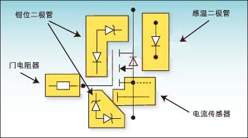
2. The error of the temperature coefficient value Sf; 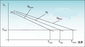
Wood Diffuser PRECAUTIONS, please read below to avoid any malfunction to the unit: