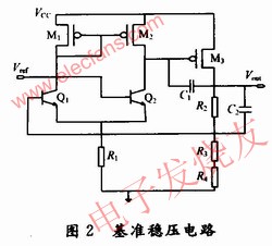
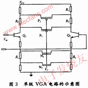
0 Preface The variable gain amplifier (VGA) can realize the amplification of input signals of different amplitudes, and is widely used in a wide input dynamic range system such as a disk reading drive circuit and a TV tuner. In the analog front end of the wireless signal transceiver and the communication AGC system, it also plays a vital role. Common VGA forms are diverse. The gain is changed by changing the equivalent transconductance of the amplifier, that is, changing the magnitude of the signal current flowing into the load, such as the Gilhert structure circuit, but its fully differential circuit stacks multiple layers of tubes, limiting the output dynamic range. The output resistance can be simply changed, but at this time the output node is the main pole of the amplifier, and the change of the output resistance will cause the bandwidth to change greatly. Recently, there are many circuits with exponentially regular VGA structures, but the circuits are relatively complicated. This paper constructs a new circuit structure consisting of a voltage stabilizing source, a VGA, and a control circuit for a pre-variable gain amplifier in a super-heterodyne TV IF receiver chip. Starting from the key indicators such as power supply voltage, dynamic range, and bandwidth, the circuit has the characteristics of high gain and large bandwidth, and ensures good linearity. In addition, noise distribution is also considered in the design of the control circuit, and the signal-to-noise ratio of the circuit is improved. . The structural block diagram is shown as in Fig. 1. 1 Circuit design and analysis 1.1 Voltage regulator circuit In order to avoid the influence of external power supply fluctuations and temperature changes on the voltage across the drain source of the MOS tube and improve the accuracy of gain control, each level of VGA design is equipped with an independent voltage regulator source. The voltage regulation process is a negative feedback process, which utilizes the adjustment of the transconductance of the adjustment tube to maintain the output within a certain range, as shown in Figure 2. In Fig. 2, Q1 and Q2 constitute a comparator, and M3 is a regulating tube. When the external power supply disturbance or load change makes Vout increase, the increase of Vout is obtained by sampling through resistors R2 ~ R4. The value of Vref-Vbl decreases, the output of the comparator decreases, and the transconductance gm3 becomes smaller, forcing Vout to decrease, so that the output is stable Reference voltage. in working: To eliminate amplifier self-excitation, add C1 = C2 = 1.25 pF to the circuit. C1 is connected across the amplifier M3 to form Miller compensation; C2 is connected in parallel with R2 in the feedback loop to form lead compensation, which effectively guarantees that the phase margin is greater than 45 ° and improves the stability of the feedback circuit. In addition, the size of the adjustment tube M3 is increased, so that (W / L) 3 = 10 (W / L) 1,2, to ensure that there is sufficient margin for the limit parameters in the worst case to ensure the normal operation of the circuit. 1.2 VGA circuit The literature simply adopts the structure that the polysilicon resistance and the MOS tube are connected in parallel, and the gate voltage is used to change the output resistance value. In order to improve linearity and controllability, this paper adopts the coexistence structure of output resistance and emitter resistance, respectively connecting different size pipes P1 ~ P5, N1 ~ N6 in parallel, the structure is simplified as shown in Figure 3. In Figure 3: (W / L) P2> (W / L) P1, (W / L) N2> (W / L) N1 Take the N tube as an example when the circuit is working: start Vc = 0, then Vgs-Vth <0, all N tubes are cut off. When Vc rises to just 0 In parallel with the emitter, the emitter resistance Rs is reduced. When the control voltage Vc continues to rise, the N1 tube is turned on, and Rs further decreases. By selecting the tube width to length ratio, to ensure the parallel resistance Ron2 When Vc increases, N tubes turn on one by one, Rs decreases, P tubes turn off one by one, Rc becomes larger, and Av becomes larger. Because Vc controls Rc and Rs to change simultaneously, it is possible to achieve a larger output dynamic range change under a smaller range of control conditions. 1.3 Control circuit In order to reduce the noise figure and adjust the gain range as much as possible, the following circuit is designed to generate mutually delayed control voltages V1 and V2, which are controlled from the second and third stages to ensure that the first stage is at a larger gain. As shown in Figure 4. C1 and C2 are charged through Q5 and Q4, respectively, so that Vc1 = Vc2 = Vb = 4 V. When Iin> O, the two channels form a discharge loop with the current mirror formed by Q8 and Q7, respectively, and control the voltage value of the capacitor. The capacitor voltage is: P1 and P2 form a current mirror to charge C1 to reduce the impact of the shunt. When Iin is small, V1 can remain basically unchanged and produce a delay effect. The current mirror is as follows: When Iin is large enough, the capacitor voltage drops through diodes Q5 and Q4, and is kept at about 0.7V. In order to control the input current in a certain range, you can choose the appropriate resistance ratio and current mirror size. The bias circuit is not shown. 2 Layout design and simulation results Use HSpice circuit simulation software to simulate under UMC 0.5μmBiCMOS process library. Perform a DC analysis of the control circuit at Vb = 4 V. Figure 5 shows the relationship between the control voltage and the input current. It can be seen from the figure that when there is no discharge loop, C1 and C2 are charged at Vb = 4 V, when 0V2; when 30μA When the gain is not large, it can be obtained by the second and third stage adjustment. When the gain requirement is higher, the first stage starts to control, so as to increase the total gain range of the amplifier and achieve the purpose of wide range adjustment. The gain has good linearity in the range of 66 dB, see Figure 6. Figure 7 shows the frequency response of the circuit at five different input currents. When the input current is 0, the amplifier is at 66 dB at the maximum gain; the input current increases, the control voltage decreases, and the gain decreases; when the input current exceeds 60 μA, Av drops to about 0 dB. The total gain change is inversely proportional to the input current. The noise figure simulation does not exceed 28 dB. Gain distribution is critical to the receiver, and the design requires a maximum gain of 60 dB. This article uses three-stage differential amplifiers connected in series, each stage control range is about 20 dB, the highest 66 dB, the minimum bandwidth is 15 ~ 88 MHz, meet the design specifications, see Table 1. 3 Conclusion Aiming at the design needs of an intermediate frequency receiver chip, this paper proposes a wide-range VGA circuit. Through the control and voltage regulation module, the gain dynamic range and circuit stability are further improved. The simulation results show that the amplifier achieves a 66 dB gain linear wide-range adjustment under 70 μA control conditions, the performance meets the indicators, and can be put into actual production. This circuit is also suitable for other wide-range VGA applications. Two-axis phone stabilizer is composed of rolling axis and tilt-axis. With a gyro-stabilized gimbal system, it reduces the movements when you are moving to shoot a smooth video. Two-axis Smartphone Stabilizer Two-Axis Smartphone Stabilizer,Popular Two-Axis Smartphone Stabilizer,Professional Two-Axis Smartphone Stabilizer,Handheld Two-Axis Smartphone Stabilizer GUANGZHOU WEWOW ELECTRONIC CO., LTD. , https://www.stabilizers.pl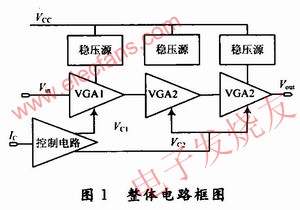


![]()


![]()


2 axis gimbal stabilizer is compatible with various smartphone.
Wewow focusing on handheld stabilizer is a technology company which does R & D independently. With Wenpod series product released, the company achieved the industry's praise and quickly became the leader of the smart stabilizer industry.
Our service
1. Reply to you within 24 hours.
2. Already sample: within 1-2days.
3. Shipping date: within 24 hours once get the payment.
4. 12 months warranty.
5. After-sales service, solve within 3 working dates.
If you have any questions, please contact with us directly.
Wewow appreciates domestic and international business relationship!