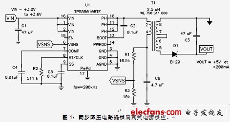
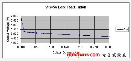
This article will discuss how to design an isolated power supply circuit for gate drive, isolated sensing and communication circuits with the least parts, the least complexity and the most cost-effective method. This circuit can be used when the input voltage is low and the circuit is energized with a slight (5%) voltage deviation. The example in Figure 1 demonstrates an IC specifically developed for a simple isolated bias power supply. Any synchronous buck circuit that allows sink operaton can be used. This circuit is called an asymmetrical half-bridge flybuck (asymmetrical half-bridge flybuck), and its operation is quite similar to a synchronous buck regulator. The output of the FET totem pole connected to the input voltage supplies the inductive capacitance filter. Next, the filter output is adjusted through the voltage divider and the negative input of the error amplifier. The error amplifier controls the duty cycle of the FET totem pole output to maintain the DC voltage at the sense point. The voltage of C6 is equivalent to the duty factor multiplied by the input voltage. As with the buck power level, the voltage-second of the inductor must be equal to zero. But this circuit adds a coupled winding to the inductor, and uses a diode to correct the reflected inductor voltage when the low-level FET starts up. Since the inductor voltage during this period is equal to the output voltage, the output of the circuit will be regulated. However, the difference in voltage drop between the primary and secondary sides will reduce the effect of regulation. In this circuit, the voltage regulation of the load will be affected by the forward voltage drop of diode D1. If the diode is changed to an FET, the effect of load regulation can be improved. Figure 1: The synchronous buck circuit provides an isolated power supply. Like the coupled inductor SEPIC, this topological parasitic component also affects circuit performance. During the on-time, the circuit is in good condition, and most of the current flows into the magnetizing inductance of the coupling inductor T1, charging C6. The output capacitor C3 supplies the load current. However, during shutdown, the two capacitors will be placed in parallel through the coupled winding of the inductor. The two capacitors have different voltages, and only the parasitic components in the loop will limit the current between the two. These parasitic components include the ESR of these two capacitors, the winding resistance of the coupled inductor, the impedance of the low-level MOSFET and diode, and the leakage inductance of the coupled inductor. Figure 2 shows the simulated current for different leakage inductance values. The upper half is the current on the primary side of T1, and the lower half is the current on the output diode D1. The leakage inductance of the tightly coupled inductor 10 nH and the loosely coupled inductor 1 uH are different. For tightly coupled inductors, the peak current is higher, which is also substantially limited by the loop impedance. For loosely coupled inductors, the peak current is lower. Higher leakage loss reduces RMS current and helps improve the efficiency of power supply. Figure 2 shows a comparison of the two. The current of loosely coupled inductors can be reduced by up to 50%, and the loss of a few components can be reduced by 75%. The disadvantage of loose coupling is poor regulation of the output voltage. Figure 2: Low leakage increases circulating current. Figure 3 shows the load regulation results presented by the converter shown in Figure 1. If the load current is limited, in most cases, this converter will provide sufficient regulation. At light load, it can be seen that the diode junction voltage changes and ringing. A minimum load or Zener clamp may be required to reduce these light load effects. Under heavy load, the parasitic components of the circuit will reduce the effect of regulation. Therefore, reducing the number of components helps to improve the effect. For example, changing the diode to synchronous switching will greatly improve load regulation. Figure 3: Flyback load regulation is good in most cases. All in all, the flyback converter is a very attractive topology, can provide a low-cost and simple isolated power supply, withstand 5% to 10% output voltage changes. The output efficiency of the diode rectifier at 5V can maintain a good state of 80%, and the state of the synchronous rectifier will also be improved. Solar Led Street Light,High Quality Solar Led Street Light,Solar Led Street Light Details, CN ZHONGSHAN G-LIGHTS LIGHTING CO., LTD. , https://www.glightsled.com