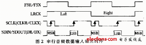
The audio delayer can be used for live broadcasting of radio stations. It delays the audio signal to be broadcast for a period of time to avoid the host ’s mistakes or some unhealthy comments of the listeners in the listener hotline through the broadcast media, thereby achieving the safe broadcast of live broadcasts Out. As broadcast-grade equipment, audio delay devices have high requirements on performance indicators such as dynamic range, distortion, signal-to-noise ratio, and frequency response, so digital technology is generally used. The computer's built-in full-duplex sound card hard disk can be used to achieve audio signal blinking in software, but it is inconvenient to use and operate, with poor reliability and low performance and price. The broadcast-grade digital audio delay device based on high-precision Σ-ΔADC and DSP chip proposed in this paper has the characteristics of high performance index, easy operation and complete functions. The design has been commercialized. 1 System structure 1.1 System configuration The hardware of the delay device is a master-slave structure, as shown in Figure 1, which is mainly composed of a single-chip M68HC05C8, DSP chip TMS320C32 and audio codec CS4224. M68HC05C8 as the host of the entire system, complete the control function of the system. As the core of the system, TMS320C32 completes the delay function of audio signals. The CS4224 and the audio input and output conditioning circuit work together to complete the A / D and D / A conversion of the audio signal. CS4224 is a high-performance 24-bit audio codec that uses ∑-Δ technology to provide full-duplex stereo digital-to-analog and analog-to-digital conversion, with a dynamic range of 105dB, harmonic distortion and manipulation of -97dB, and a sampling frequency of 32kHz , 44.1kHz and 48kHz are optional. The chip uses differential input and output, on-chip anti-aliasing filter and output smoothing filter and digital de-emphasis filter circuit, with analog volume control, support master or slave working mode. TMS320C32 is a low-cost, high-performance floating-point DSP chip, very suitable for voice digital signal processing. It supports 24-bit address bus and 32-bit data bus, and can address the large-capacity memory required by the delayer. It also has a serial interface to facilitate the CS4224 interface for serial audio data input and output. M68HC05C8 realizes the man-machine interface, manages the keyboard display and delayer remote control interface, and controls the operation of CS4224 and TMS320C32. 1.2 Memory interface TMS320C32 has an enhanced external memory interface, the width of the program memory can be 16 and 32 bits, and the data memory can be three widths of 8/16/32 bits. TMS320C32 uses two sets of strobe signals STRB1 and STRB0, which have different addressing ranges. Each group of strobe signals consists of four pins, which serve as chip selects and additional address lines. The characteristics of the pins are determined by the bus control register corresponding to each group of strobe signals. By setting certain fields of the bus control register, you can specify the data type and the width of the external memory. The delay uses two sets of memories with different widths. SRAM stores audio data, set the memory width to 32 bits, and the data type to 32 bits. Since the audio codec CS4224 is 24 bits, it actually uses 24 bits and is composed of three 8-bit SRAMs, which are respectively selected with STRB0_B0 ~ 2. The FLASH chip 28F512 stores the user audio signal processing program, the memory width is 8 bits, and the chip selection is ATRB1_B0. The memory interface mainly considers the memory speed to determine how many wait states need to be inserted. Because the clock frequency of TMS320C32 is 40MHz, and the access speed of FLASH memory is 150ns, the access speed of SRAM is 70ns, so it must be inserted into the wait state. TMS320C32 has an internal programmable software wait state generator, selects the working mode of the wait state generator through the SWW field of the STRBx control register, and writes the number of machine cycles to wait in the WTCNT field. Since STRB1 and STRB0 strobes are used for program memory and data storage, respectively, the required number of machine cycles can be set according to their respective access speeds. TMS320C32 has program guide function. When the hardware reset makes the MCBL / MP pin high, it works in microcomputer mode, executes the on-chip boot program, and loads the user program in the FLASH memory into the internal high-speed RAM to run. The boot mode can be determined by INT0 ~ 3 of the pin. The load address of the external memory is selected as the Boot3 area according to the connection mode of the memory, and the handshake signal is not used. The front end of the FLASH memory is the program header, including the necessary information for the TMS320C32 at boot, such as the width of the external memory, the contents of the bus control register after the boot, the length of each data block, the width of the target memory, and the data type. 1.3 Audio data interface CS4224 and TMS320C32 are connected in serial mode. The serial data lines SDIN and SDOUT of the CS4224 are directly connected to the serial data lines DR and DX of the TMS320C32 respectively. The data shift clock SCLK is connected to the data transceiver clocks CLKX and CLKR. Clock FSX and FSR. See Figure 2 for working timing. The TMS320C23 serial port can work in variable or fixed data rate mode for continuous or burst transmission. The delayer selects variable data rate mode and burst transmission, and works at the highest frame rate, that is, there is no pause between the previous frame and the following frame. 1.4 Control interface The CS4224 can be controlled by two interface methods: SPI and I2C, and selected by the pin SPI / I2C. The delayer adopts SPI mode to control the working mode of CS4224. CS, CDIN and CCLK are chip select, data line and bit clock respectively, controlled by the built-in SPI interface of M68HC05C8. Given the address of the CS4224 control register, the microcontroller can read and write the contents of the control register. M68HC05C8 resets CS4224 through port PC6. The I / O lines provided by the TMS320C32 chip itself are only XF0 and XF1. These two lines are used to send data and receive data lines, respectively, to form an asynchronous serial port, and communicate with the M68HC05C8 through the software module. The MMS controls the TMS320C32 Running. At the same time, the microcontroller controls the reset terminal of TMS320C32, the working mode selection terminal MCBL / MP and the boot mode selection terminal INT0 ~ 3 through ports PC0 ~ 5. The fast Ethernet POE Switch supports 60-watt PoE budget to power up to 4 IEEE 802.3af (or 2 IEEE 802.3 at) compliant powered devices simultaneously. The PoE features make fast Ethernet POE switch an efficient and cost-effective solution for SMB, SOHO or other similar fields where there is deployment of PoE network for the wireless access points, IP-based surveillance cameras or IP phones anywhere else. Fast Ethernet POE Switch,4 Ports Ethernet POE Switch,Small Fast Ethernet POE Switch,8 Ports Ethernet POE Switch,10/100M POE Switch, POE Switch 10/100M Shenzhen N-net High-Tech Co.,Ltd , http://www.nnetswitch.com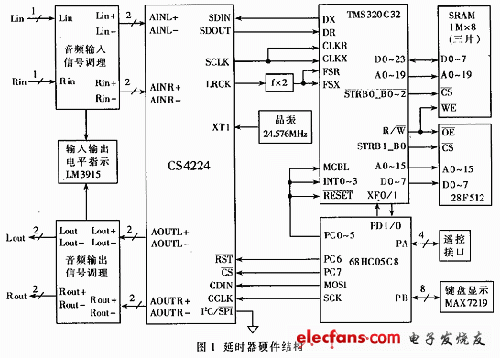
To satisfy the increasing demand of PoE for Fast Ethernet (FE) networking, N-net has developed this series of PoE FE switch.