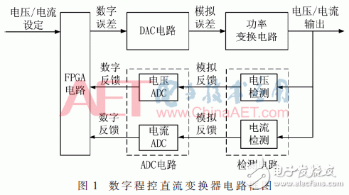
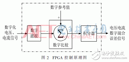
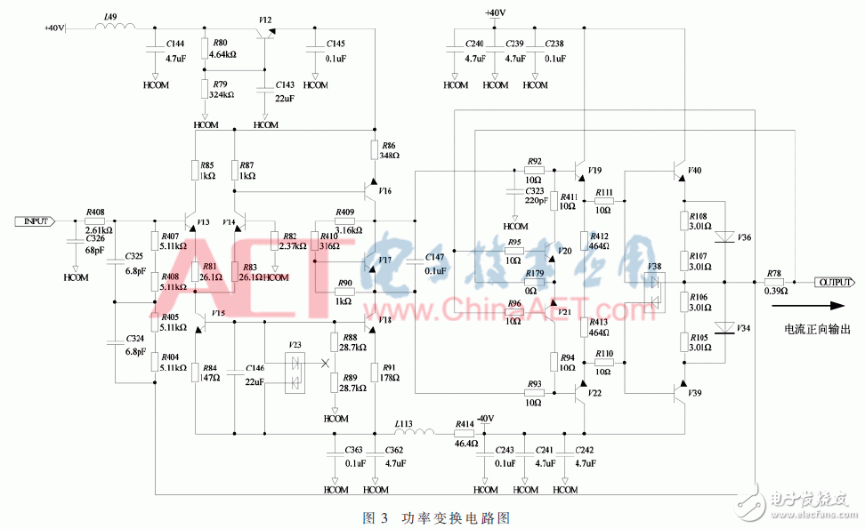
The rapid development of precision instruments has placed increasing demands on the quality of DC converters. In order to obtain stable high-performance DC output, a digital programmable DC converter with FPGA as the core is proposed. The overall scheme of the converter is introduced, and the main hardware circuit and software design are given. The experimental results show that the converter has the characteristics of high output precision, small ripple, good stability and high reliability, which can meet the requirements of electronic measurement field. The traditional converter uses analog hardware to implement closed-loop feedback control to obtain stable voltage and current output. The simulation controls the state of the real-time reaction system, and the response speed is fast. However, in the field of test technology and instrument products, the stability of the simulation system cannot meet the actual needs. In order to achieve high stability, a large number of components need to be added for loop compensation. Moreover, factors such as load, environmental changes, and parasitic parameters, drift, aging, and inconsistency of components in the feedback loop affect the stability of the system to some extent [1, 2]. Therefore, in a high-performance converter system that requires a faster real-time response speed, it is difficult to achieve a good transient response to complex changes in input voltage and load by analog control, and stable control in multiple states cannot be obtained. With the rapid development of integrated circuit manufacturing technology, a large number of programmable digital chips and microprocessors have been introduced, and digital control converters have begun to attract people's attention. DC converters have entered the era of digital converters from the era of analog converters [3, 4]. The core of digital control technology is that the digital closed-loop control algorithm is completed by software configuration, which greatly reduces the use of analog devices, reduces the complexity of hardware systems, achieves accurate nonlinear control, and avoids system instability due to device parameter changes and failures. degree. At the same time, the digital filter is used in the system to realize the zero-pole automatic compensation function of the control loop, which greatly improves the loop control performance. In the field of digital DC converters, the more mature control chips are mainly MCUs or DSPs. However, due to the limited speed [5, 6], scholars have begun to shift their focus to FPGAs, such as the literature [7-9]. However, the core of the literature [7-9] lies in the pulse width modulation technology. This paper proposes a new design scheme, and studies a program-controlled DC converter that implements digital control technology using FPGA to achieve high-stability voltage and current output. 1.1 System Design Compared with the traditional analog loop control DC converter, the digitally controlled DC converter has high stability, reliability and flexibility, and can adapt to more complex dynamic loads. The circuit block diagram of the digital program-controlled DC converter is shown in Figure 1. It consists of five basic circuit blocks, namely FPGA circuit, digital-to-analog conversion DAC circuit, power conversion circuit, detection circuit and analog-to-digital conversion ADC circuit. The FPGA circuit is used as a digital DC converter control core device to realize voltage closed-loop control and current closed-loop control. The detection circuit collects the output voltage and current signals of the converter, converts them into digital feedback signals through the ADC circuit, and sends them to the FPGA for digital signal processing, which is compared with the digital set values ​​of voltage and current. After the digital processing of the FPGA, the output voltage and current digital mixing error is converted into analog error by a DAC circuit, and the power conversion circuit is entered to complete the nonlinear accurate output of the voltage and current signals. 1.2 FPGA design The FPGA selects XC3S2000-5FGG456C chip of XILINX company. This device not only has rich clock resources and I/O resources, but also has good repeatable erasing performance, simple debugging and convenient programming, which can well meet the needs of this paper. The FPGA control principle is shown in Figure 2, including digital filtering, digital comparison and digital integration. The digital filter and integrator are configured by the user according to the load. The DC accuracy and output response are adjusted by changing the integral time constant. The digital filter is also a custom-compensated zero-pole filter that changes the phase of the system to avoid overvoltage surges and oscillations due to fast system response. Digital filtering and digital integration form the overall response of the system, and digital filters and integrators can be customized for different load characteristics to achieve the desired DC output. 2.1 Power Conversion Circuit Design The power conversion circuit is the focus of the hardware circuit design in this paper. It mainly performs energy conversion for power output or absorption power, but at the same time affects the output ripple, noise, conversion efficiency and stability of the converter. The circuit diagram is shown in the figure. 3 is shown. V12, R79, R80, C143, and C145 form an active filter with a voltage regulation function. Using the current amplification of V12, the base ripple suppression capability is amplified, the capacity of the filter capacitor is greatly reduced, and the filtering effect of the circuit is significantly improved. V13 and V14 are differential pair tubes, and form a single-input and single-out differential amplifier circuit with R81, R82, R83, R85 and R86. The V13 base signal is converted into V14 collector signal output and sent to the V16 base. V15, V18, V23, R84, R88, R89, R91, C146 form a constant current source circuit to improve the input impedance of the amplifier circuit, and at the same time suppress the common mode signal and provide current. V23 is a double diode, which provides V15 and V18. The voltage is biased and the constant current value is set by R84 and R91. V16 and R86 form a common emitter amplification circuit that maps the V13 base signal change. V17, R90, R409 and R410 form a VBE expansion circuit, which functions to provide appropriate DC offset for V19 and V22 to eliminate V19, V22 crossover distortion. The dual diode V38 provides an appropriate bias voltage to V39 and V40 to ensure that V39 and V40 are in a micro-conduction state to prevent crossover distortion of V39 and V40. V20, V21, R78, R95, R96 and R179 form a bidirectional current protection circuit, and R78 is a current monitoring resistor. By controlling the voltage difference between the two ends, V20 and V21 are controlled to be turned on and off. Once the forward output is overcurrent, the voltage across R78 is greater than the BE junction voltage of V20, V20 is turned on, V19 and V40 are turned off, and the output is limited; otherwise, the reverse output is overcurrent, and the voltage across R78 is greater than V21 BE junction voltage, V21 Turned on, V22, V39 are turned off, and the output is limited. R404, R405, R406, R407, C324, C325 lead the output signal back to the input, providing negative feedback for the power conversion circuit, ensuring that the control loop is stable and effectively suppressing output noise. 2.2 DAC circuit design Idc Connectors,Idc Socket Connector,Idc Electronic Socket Connector,2.00Mm Socket Connector Dongguan Yangyue Metal Technology Co., Ltd , https://www.yyconnector.com