1 Introduction Most medical ultrasonic diagnostic imaging techniques use the ultrasonic pulse echo method, which uses a probe to generate ultrasound waves into the human body. The echoes generated by the reflection of human tissue are converted into electrical signals after being received by the transducer, and then extracted, amplified, processed, and then The digital scan converter is converted into a standard video signal, and finally displayed by the display. In the fully digital B-mode ultrasound system based on FPGA + ARM 9 hardware platform, the echo signal returned by the front-end probe needs to be beam synthesized, related processed, collected and transmitted to the ARM embedded processing system by the real-time acquisition system, and the video signal data Large volume and high real-time requirements, so FPGA + SRAM is used to form a real-time acquisition system, which can meet the above requirements in speed and capacity. This paper mainly introduces the principle and realization of the use of FPGA for logical control of ultrasound video image acquisition in B-mode imaging system. 2. Working principle of system composition As shown in Figure 1, the acquisition system first uses a digital beam synthesizer to synthesize the multi-channel ultrasonic echo signals. The digital beam synthesizer delays the signals of different channels so that the signals at the same point are added in phase and simultaneously The echo signal of the channel is windowed in the spatial domain, similar to matched filtering, which can improve the signal-to-noise ratio of the signal. Then, the synthesized ultrasonic video signal is subjected to a frame-related preprocessing, that is, a smoothing process on the corresponding pixel gray level between the image frame and the frame. Because the noise superimposed on the image is uncorrelated and has zero mean random noise, if the average value of several frames is taken to replace the original image under the same conditions, the noise intensity can be reduced. In the frame-related process, FPGA should control the reading, processing and storage of data. In order to meet the real-time nature of the video display, the acquisition system uses a ping-pong mechanism with a dual-frame storage structure, and the FPGA implements read-write interlock control. After the frame-related processing, the video data is alternately written into frame storage A and frame storage B. The frame storage read controller reads the data in the frame storage according to the back-end processing speed and sends it to the DMA controller. The DMA controller opens the DMA channel Perform data transfer. When FPGA implements read and write control, in order to avoid reading and writing to a frame store at the same time, it is necessary to set a read-write mutual exclusion lock to switch the memory state. 3.1 Digital beam synthesis For the ultrasonic probe with 128 elements and 32 transceiver channels, after 32 AD conversions, it is divided into 4 groups, each group has 8 receiving channels, and each group is implemented with an FPGA. Time and dynamic focus then perform weighted summation, and then summation between groups to generate an ultrasound digital video signal. The system block diagram of each group is shown in Figure 2: 3.2 Frame related processing The frame correlation module is shown in Fig. 3, which is composed of a frame correlation controller and a piece of memory. The frame correlation memory uses a static memory (SRAM) with a size of 256 kB. The frame-related controller is implemented by FPGA, which completes the address generation, memory read and write control, and frame-related calculation functions. Because of the real-time requirements, that is to ensure that the data sent to the back-end dual-frame storage cannot be interrupted, so consider the pixel-by-pixel data Related processing is performed at the same time of reading and writing, and it needs to be completed within the same pixel clock cycle. The read / write controller needs to read out the data in the memory and the current frame data in the first half of a pixel clock cycle for related processing; the second half of the clock cycle then writes the relevant processed data into the memory for later use, In this way, the data sent to the back-end dual-frame storage is still continuous pixel data corresponding to the pixel clock. The frame-related workflow is as follows: (1) Address generation. The address is generated by a pixel counter, and the input signals are the frame synchronization signal VS and the pixel clock CLK. The frame synchronization signal VS provided by the front end is the reset signal of the counter. At the beginning of each frame, the counter is cleared, and then the address is generated according to the count of the pixel clock CLK. The address does not change within each pixel clock cycle, and is performed according to this address Memory reading and writing. (2) Read existing data and related processing. In the first half of a pixel clock cycle, that is, when CLK jumps to a high level, the read signal OEl output by the read and write controller is valid, and the data of one pixel in the previous frame is read out and sent to the FPGA for addition. The A port of the device is added to the corresponding pixel data of the current frame that arrives at the B port at the same time. (3) Data storage and transmission. In the second half of the same pixel clock cycle, that is, when CLK jumps to low level, the write signal WE1 output by the read and write controller is valid, and the relevant processed data is written back to the original address, and the data is also sent Write control module to frame storage. Ultrasound video images need to be collected in real time and reconstructed on the display after processing. The image memory must continuously write data, and at the same time, it must continuously read data from the memory and send it to the back-end for processing and display. In addition, in order to meet this requirement, you can set up two pieces of frame storage with the same capacity in the collection system and manage them through the ping-pong read-write mechanism. The structure is shown in Figure 3. In order to ensure that at any time, only one frame is in write state, set a write mutex; at the same time, only one frame is in read state, set a read mutex. At the initial stage of the system, one frame is saved as a write-awaited state, and the other one is in a read-awaited state; after starting work, the two slices are in the process of reading and writing in turn, the conversion process is the same, but the two slices are staggered This can ensure that data can be continuously written to and read from the frame store. The mechanism is shown in Figure 4, and the workflow is: (2) The frame storage and write controller receives a frame start signal and determines that the acquisition is started, sets the frame storage A write signal WE2 A to be effective, and the frame storage A starts to write the current frame data; at the same time, the frame storage and read controller sets the frame storage B The read signal OE2_B is valid, and the frame save B starts to read the stored data; (3) At the end of a frame, the writing of the frame storage A ends and the write mutex is released; the reading of the frame storage B ends and the read and read exclusion lock is released (4) Wait for the start of another frame, the frame store A obtains the read mutex; the frame store B obtains the write read exclusive lock; (5) At the beginning of another frame, the write controller sets the frame store B write signal WE2B to be effective, and the frame store B starts to write data; the read controller sets the frame store A to read signal OE2 A to be active, and the frame store A starts to read data. 3.4 DMA transfer For the entire B-mode ultrasound system, the system must complete the real-time collection and designated processing of video image data. The processing capacity of the high-performance ARM processor can reach millions of instructions per second, so the data transmission design is to increase the system speed Key link. ARM processing system and external data transmission can be achieved by the method of CPU accessing external memory, but the efficiency is low and it cannot meet the real-time requirements of the system. The advantages of DMA data transmission are that it does not occupy CPU time and single cycle throughput rate It is widely used in real-time video image acquisition system. However, because the DMA transfer rate does not match the front-end video image data input rate, it is difficult to take advantage of DMA data transfer. The dual-frame memory composed of programmable FPGA-controlled SRAM can solve this problem well; in addition, a certain amount of RAM is embedded in the FPGA, which can be configured as a buffer memory, and the input and output can be easily realized through a flexible logic structure The control of data flow becomes the link and bridge connecting ARM processing system and SRAM. 4. Conclusion Using FPGA as the acquisition control part in the B-ultrasonic digital video image real-time acquisition system can first increase the speed of system processing and the flexibility and adaptability of the system: because SRAM is used as data buffer between FPGA and ARM processing system, and DMA The method of transmission greatly improves the performance of the system; due to the use of FPGA programmable logic devices, for different ultrasound video signals, as long as the control logic is slightly modified in the FPGA, the signal acquisition can be achieved; the peripheral hardware circuit of FPGA is simple, so In hardware design, the complexity of hardware design can be greatly reduced. The timing logic debugging of FPGA can be simulated on software, which reduces the difficulty of hardware debugging. Base site lead-acid battery protector system is the smart resonance pulse technique for 6V/36V cell battery or 6V/36V battery pack in series with 3PCS 2V/12V cells. It is working as a new generation of high-tech products for daily battery maintenance in telecom base site or electrical power system. Base Site Battery Protector System Base Site Battery Protector System,Stationary Battery Protector System,Online Battery Smart Protector System,Telecom Base Site Battery Protect System Shenzhen Daceen Technology Co., Ltd. , https://www.daceen-sz.com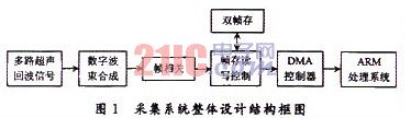
3. System design and implementation 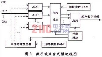
Different delays on the echo signals of different channels are the key to achieving beam focusing. The delay can be divided into coarse delay and fine delay according to accuracy: coarse delay is used to control the start time of A / D sampling, and the accuracy is 32 ns, the delay parameters are read from the on-chip RAM of the FPGA, and the system controller writes the corresponding data to these RAMs when the probe is replaced; the fine delay is generated by the sampling clock generator according to different channels. The phases of these clocks are staggered from each other, and the staggered value is just equal to the difference in propagation delay of each array element. Considering the real-time nature of the system and the change in depth during the detection process, dynamic focusing is required. Dynamic focusing is achieved after the A / D sampling starts, by reading the dynamic focusing parameters, and controlling the sampling clock generator during the sampling process.
The echo signals of the 8 channels are sampled by A / D and then sent to the FPGA. After buffering, they are synchronously read out and enter the weighting module. The weighting module consists of 8 unsigned digital multipliers. Echo signals are multiplied by weighting parameters to obtain data with dynamic focusing and weighting characteristics. The 8 sets of data then pass through the 3-level adder to obtain the ultrasonic digital video data after beam synthesis. 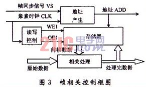
3.3 Frame storage ping-pong read-write control mechanism 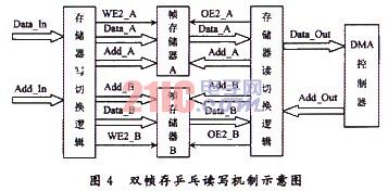
(1) The collection process is not started, frame storage A is in the state of waiting for writing, and the write mutex is obtained; frame storage B is in the state of waiting for reading, and the read mutex is obtained;
It utilizes the energy from battery self-power or floating power supply, to produce a unique smart electronic pulse, then feed back to the battery through the output line, Resonance with coarse and hard lead sulfated crystals in negative plates of batteries and converted to active substance under the reaction of pulse charging current which dissolve lead sulfated crystals, Keeping the battery working at a high efficiency. Under the disturbance by the smart resonance pulse, the new lead sulfate crystal is prevented from being formed, and the service lifespan of the lead-acid battery is prolonged 1~2 times than before.
There will be individual differences in State-Of-Capacity (SOC) and internal resistance (IR Value) of batteries after used for a certain number of years. It is called the battery unbalancing. Due to the total floating charge voltage of the rectifier remains unchanged and keeps constant, when the battery pack is in floating charging status, the floating voltage of the cells with larger internal resistance will be higher than that of the normal battery, resulting in the normal battery's floating voltage is lower. Batteries floating charged in this unbalancing way for a long time will cause the higher voltage cells seriously water dehydrated, and the lower voltage cell is in a state of under charged. This way of vicious spiral formed will accelerate the base site batteries premature failure.
Our protector system set a equalized charging function. If the terminal floating voltage of the battery system is higher than the standard value of protector system designed, the system automatically and smartly switches to the over-voltage balanced working state. When the voltage drops lower than standard value, it automatically changes to smart pulse maintaining state. The decrease of battery internal resistance and the improvement of the battery equalization lead to the battery lifespan prolonged.
Principle and Realization of Image Acquisition of B-mode Ultrasound System Based on FPGA
Principle and Realization of Image Acquisition of B-mode Ultrasound System Based on FPGA