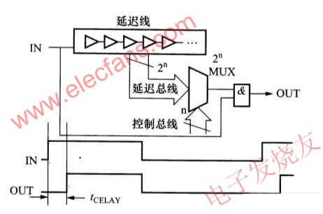
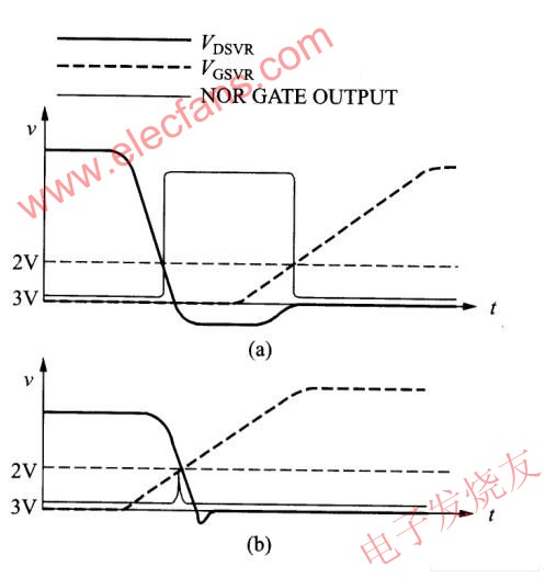
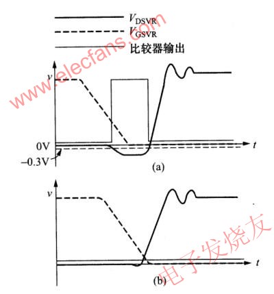
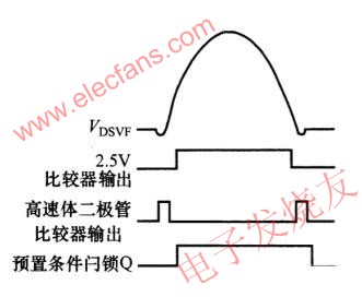
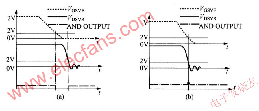
To reduce conduction loss and reverse recovery loss, synchronous rectification requires an accurate time control circuit. Although there are several methods to generate control signals, we now use a gate drive signal timing that is actively controlled from a feedback system system. The key advantage is that the circuit will specifically adjust the uncontrollable capacitance in the synchronous rectification MOSFET according to the change of the component state. The influence of time delay and temperature change on the MOSFET threshold can be corrected according to the feedback loop. In order to control the time of the gate movement, an adjustable delay circuit is used in FIG. 1. The delay circuit contains three main components, a delay line, a multiplier, and a logic AND gate circuit. The input signal to the delay line is a signal delayed by several nanoseconds relative to each delay element. To generate a delay that controls conduction, the multiplier selects the element that delays the output signal, and finally the AND gate determines that the delay is added to the rising edge of the drive conduction. The delay control from IN to OUT is performed by the digital control bus, which is added to the address input of the multiplier. Conversely, if the control bus is set to all 0s, the delay from IN to OUT is 0, that is, there is no delay. Several different delay times can be set, giving several kinds of turn-on delay time, turn-off delay time, or symmetric turn-on and turn-off delay. Note that in Figure 1 is a voltage detection circuit and digital controller. In order to perform different delay settings, different voltage detection circuits and digital controllers are used. Figure 1 Adjustable delay circuit A. Controlling the execution plan of driving VR The design of the control drive circuit starts with the reflowed MOSFET VR. As its source-drain voltage drops to zero, it will be turned off immediately. A simple way to achieve it is to use a comparator to detect the zero-crossing time of the source-drain voltage of VR. The problem with this method is that the delay of the logic circuit and gate drive through the comparator will be generated, which should be considered. Even for very fast circuits, the total delay will be 50ns or more. During this period, the body diode will turn on and increase the large conduction loss. From detecting the dropped source-drain voltage to when the MOSFET is turned on, the inherent time delay of a logic response can be processed with the information obtained from the last switching cycle. Set the next turn-on of the MOSFET. In this expected method, the gate voltage of the MOSFET begins to increase before its source-drain voltage drops. During this period, the gate voltage is allowed to operate in advance. When the source-drain voltage drops, it turns on, and the body diode never turns on. Figure 2 shows that the control circuit can turn on and turn off the VR. It uses two multipliers, two counters, a delay line and glue logic to control the MOSFET conduction and delay, thus eliminating the conduction of the body diode. The description of the circuit begins with the turn-on delay of the MOSFET. The PWM control signal drives the primary-side MOSFET Q1 and is simultaneously added to the delay line. When the power is turned on for the first time, the LOAD input to the counter is high, it sets the counter of the on delay to all 1 (high level), and sets the counter of the off delay to all zero (low level) ), As the counter starts counting, from the output of the control circuit to the result of the gate drive is the largest on-delay and the smallest off-delay. Figure 2 VR control circuit With these values ​​set for the delay, the VR body diode will turn on, and the feedback loop will also begin to adjust the delay to achieve the minimum body diode conduction. Figures 3 (a) and (b) show that VR is conducting During the gate-source and drain-source voltages, Figure 3 (a) shows the circuit with too long delay when VR is turned on, and Figure 3 (b) shows the best delay time. Figure 3 VR opening waveform Adjust the turn-off delay, use an OR gate at an input threshold of about 2V to detect whether the gate-source voltage and the drain-source voltage of VR are both low, and the high level from the OR gate indicates the controller. If the delay time is too long, the controller will reduce the delay in the next switching cycle. The output of the OR gate is latched, inverted and sent to the UP / DOWN input of the start delay counter. This signal tells the counter to count up or down. If the OR gate output is high, the counter counts down to reduce the delay time. When the OR gate is at a low level, the counter counts up, and the delay time is increased. The counter effectively keeps the delay information for the next duty cycle. The feedback loop will adjust the opening delay to shorten it until the OR gate has no longer output pulse. When the counter works at a constant load and line voltage, the opening delay for the next cycle will be slightly longer, or the OR gate will give a high output pulse , The delay will be shortened, in this way, the circuit will jitter between two delay times, one is longer, the other will be close to the optimal state. Shutting down the controller works in a management manner very similar to turning on the controller. The difference lies in the counting direction of the voltage detection circuit and the counter. When the body diode is turned on, a high-speed comparator is used for detection. For more accuracy, a comparator is used to detect the body diode conduction and replace the OR gate. During the turn-on period, the current is commutating from the rectifier MOSFET to the return MOSFET. The current DI / DT is very high. The source-drain voltage of VR is usually You can see its ringing. If a comparator is used to detect the state of the body diode during VR conduction, false triggering may occur due to the ringing of the source-drain voltage. During VR off, the current through the VR MOSFET device is constant. This current either passes through its channel or through its body diode. At turn-off, there is only very small ringing. The comparator is used to improve accuracy. The threshold of the comparator must be a little more negative than the previous false trigger value when the MOSFET channel is turned on. During channel conduction, the source-drain voltage is approximately equal to I LOAD * .RDS (ON), and noise is specified. The comparator threshold is set at approximately -300mV. The comparator compares the source-drain voltage of VR with this set threshold. The high level from the comparator indicates to the controller that the body diode is conducting and the delay time needs to be increased, which corresponds exactly to the turn-on situation. Because the turn-off delay count is set to 0 at the beginning. Figures 4 (a) and (b) show the VR turn-off waveform and the output of the comparator. Figure 4 VR turn-off waveform (a) non-optimal delay (b) optimal delay Fig. 4 (a) shows the operating state of the circuit when the delay setting is too short. Fig. 4 (b) shows the optimal delay state. Since the turn-off delay is in a jitter state at a certain value when the VR is on, these are the two states that are too long and the optimal value. The problem arises: can the turn-on delay and turn-off delay be set shorter, will this cause cross-conduction, the problem is to carefully study the characteristics of the comparator, and the delay of each element of the delay line, the comparator can only respond to differential inputs Voltage, this voltage will only exist for a sufficient amount of time at the transition interval node. Assume that the comparator can detect the body diode conduction time of 5ns. In the next cycle, the delay can be adjusted, using a digit on the delay line to reduce the conduction of the body diode. Of course, the comparator will not respond to the turn-on of the body diode of the next cycle because it reduces the delay time by approximately 5 ns on each element of the delay line. The key measure to prevent cross-conduction is to set the delay of each element to be less than the minimum pulse width that the comparator can detect. B. Control the execution of driving QF The control of the forward rectified QF is very different from the return element VR. One major difference is that its goal is to turn on QF after the transformer is reset. It is independent of the rising and falling edges of the PWM control signal, and it is different from the reflowed MOSFET. Here, the goal is simply to adjust the time of the rising and falling edges of the PWM controller signal to reduce the on-time of the VR body diode and minimize it. Understand that the goal is to turn on QF after the transformer is reset. A good starting point is the circuit shown in Figure 5 to turn on QF. Figure 5 VR control circuit First, a high-speed body diode comparator is used to detect the body diode when QF starts to turn on. It sends a signal at the end of the transformer reset interval. As it happens, as shown in Figure 6, this comparator will also detect the primary side MOSFET Q1. After breaking, the body diode is just turned on. Use this comparator alone to turn on QF and ensure that Q1 enters turn-off time. In this way the transformer will never be allowed to reset. To prevent this, a low-speed comparator detects the source-drain voltage of QF rises to 2.5V. When the QF source-drain voltage rises above 2.5V, a preset latch adjustment is set, which will enable the output of the high-speed body diode comparator. When the QD source-drain voltage drops below the -300mV body diode comparator threshold, QF turns on immediately and sets the QF control latch. The output of the high-speed comparator goes high. The preset latch is reset immediately, and the open circuit is in the proper state during the next turn-on event. From the body diode comparator detecting the inherent delay of the conduction of the body diode, to the channel where the QF is turned on, the body diode conducts the magnetizing current of the transformer. Although in this interval, there is conduction loss in the QF body diode, but compared with this, this is already the smallest loss encountered by QF. If QF remains off during this bad time interval. To completely eliminate this loss, use the same pre-control scheme to turn on VR. Although this is theoretically possible, it will actually be quite difficult because there is no pulse edge of the PWM control signal. The system is fully reset. Figure 6 VR pre-latching waveform A counter whose output is initially set to zero controls the shutdown circuit. The counter output is all set to 0, that is, there is actually a zero delay between the falling edge of the PWM control signal and the gate-source voltage of QF. The three waveforms are shown in Figure 7 (a). Figure 7 VF turn-off waveform (a) Non-optimal delay (b) Optimal delay The AND gate in the VF turn-off circuit has more functions such as the OR gate in the VR turn-on control circuit, giving a command to the counter to directly make the counter count up or down. In the case of the VF's shutdown circuit, a high level goes directly from the AND gate to the counter to count up in the next cycle. When the counter increases a count value for the next cycle, the delay between the falling edge of the PWM controller and the gate-source voltage of VF will increase, and the output pulse from the AND gate will become narrower. This feedback effect will continue until VF The gate-source voltage and the drain-source voltage of VR can be synchronized. When the delay is optimized, the waveform is shown in Fig. 7 (b). As described in the VR control execution circuit, the circuit will jitter between two delay values, one is the optimal value and the other is slightly longer than the optimal value. Kitchen Hob,Gas Hobs,Gas Cooker Hob,Four Burner Gas Stove xunda science&technology group co.ltd , https://www.gasstove.be