Altera's MAX 10 devices are monolithic, non-volatile, low-cost programmable logic devices (PLDs) with internal memory configurable dual flash memory, user flash memory, integrated ADCs, and support for a single-chip Nios II software processor. System Management, I/O Expansion, Communication Control Panels, Automotive Electronics, Industrial Controls, and Consumer Electronics. This article describes the main benefits of Altera® MAX® 10 FPGAs, the main features, block diagrams, and component distribution of the Altera® MAX® 10 FPGA Development Kit. Diagram, circuit diagram and main components table. The main advantages of Altera® MAX® 10 FPGAs: Advantage Supporting Feature Simple and fast configuration Secure on-die flash memory enabling device configuration in less than 10 ms Flexibility and integration Single device integration PLD logic, RAM, flash memory, digital signal processing (DSP), ADC, phase-locked loop (PLL), and I/Os Small packages available from 3 mm × 3 mm Low power Sleep mode—significant standby power reduction and resumption in less than 1 ms Longer battery life—resumption from full power-off in less than 10 ms 20-year-estimated life cycle Built on TSMC's 55 nm embedded flash process technology High productivity design tools Quartus® II web edition (no cost license) Qsys system integration tool Digital Signal Processing (DSP) Builder Nios® II Embedded Design Suite (EDS)
A fiber optic slip ring is a device that allows for the transfer of data, power, and signals between two rotating objects. The ring is made up of one or more optical fibers that are used to transmit light signals. These signals can be used to send power, data, or other signals between the two objects. The fiber optic slip ring is a newer technology that has many benefits over traditional slip rings.
A fiber optic slip ring is a device that allows electric current and optical signals to pass through a rotating joint. This is often used in applications where it is necessary to transfer data or power between two stationary points while the object rotates. The fiber optic slip ring uses light rather than metal to conduct these signals, which makes it ideal for use in high-speed or hazardous environments.
When it comes to telecommunications, fiber optics are king. They're the backbone of almost every network today, and they're getting faster and more reliable all the time. That's thanks in part to a technology called fiber optic slip rings.
A fiber optic slip ring is a device used in optical communication. It is a component of many fiber optic networks and it allows for the transmission of data over long distances without losing signal quality. Fiber optic slip rings are also used to improve the performance of other optical systems.
Fiber optic slip rings are growing in popularity for rotating applications. Fiber optic slip rings provide many advantages over traditional electrical slip rings, including much smaller size, weight, and power consumption. However, fiber optic slip rings also have a few disadvantages. One disadvantage is that they can be more expensive than traditional electrical slip rings. Additionally, fiber optic cables are more fragile than electrical cables, so they can be more susceptible to damage.
When it comes to fiber optic slip rings, there are both benefits and drawbacks to consider. On the one hand, fiber optic slip rings offer a number of advantages over traditional metal contact slip rings. They are lighter in weight, which makes them easier to install and transport. They also generate less heat, making them safer to use in hazardous environments. Additionally, they provide superior performance in terms of electrical noise and signal integrity.
However, fiber optic slip rings also have some drawbacks. They are more expensive than traditional metal contact slip rings, and they can be more difficult to repair if they malfunction. Additionally, they may not be suitable for some applications due to their limited range of motion.
Fiber Optic Slip Ring,Brass Slip Ring,Fiber Optic Silp Ring,Electrical Rotary Joint Dongguan Oubaibo Technology Co., Ltd. , https://www.sliprobs.com
MAX® 10 devices are single-chip, non-volaTIle low-cost programmable logic devices (PLDs) to integrate the opTImal set of system components.
The highlights of the MAX® 10 devices include:
Internally stored dual configuraTIon flash
User flash memory
Instant on support
Integrated analog-to-digital converters (ADCs)
Single-chipNios II soft core processor support
MAX® 10 devices are the ideal soluTIon for system management, I/O expansion, communication control planes, industrial, automotive, and consumer applications.
Altera® MAX® 10 FPGA Development Kit
The Altera® MAX® 10 FPGA Development Kit provides a full featured design platform built around a 50 K logic elements (LEs) MAX 10 FPGA, optimized for system level integration with on-die analog-to-digital converter (ADC), dual- The configuration flash, and DDR3 memory interface support. The board features on-board USB-BlasterTM II, high-speed mezannine card (HSMC), and PmodTM Compatible expansion cards, high-definition multimedia interface (HDMI) output, and dual Ethernet for Industrial Ethernet applications. The MAX 10 FPGA Development Kit provides the perfect system-level prototyping solution for industrial, automotive, consumer, and many other market applications.
With this development board, you can:
Develop designs for the 10M50D, F484 package FPGA
Measure the performance of the MAX 10 FPGA analog-to-digital block conversion
Interface MAX 10 FPGAs to DDR3 memory at 300 MHz performance
Run embedded Linux using the Nios® II processor
Interface to daughtercards and peripherals using HSMC and DigilentPmodTM Compatible connectors
Measure FPGA power (VCC_CORE and VCC_IO) using the power monitor graphical user interface (GUI)
Reuse the kit's PCB board and schematic as a model for your design
The MAX 10 FPGA Development Kit includes the following:
RoHS- and CE-compliant MAX 10 FPGA development board
Featured devices
MAX 10 FPGA (10M50D, dual supply, F484 package)
Enpirion® EN2342QI 4A PowerSoC voltage-mode synchronous step-down converter with integrated inductor
Enpirion EN6337QA 3A high-efficiency PowerSoC DC-DC step-down converters with integrated inductor
Enpirion EP5358xUI 600 mA PowerSoC DC-DC step-down converters with integrated inductor
MAX II CPLD – EPM1270M256C4N (On-board USB-Blaster II)
Programming and Configuration
Embedded USB-Blaster II (JTAG)
Optional JTAG direct via 10-pin header
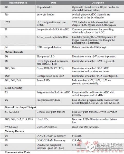
Memory devices
64Mx16 1 Gb DDR3 SDRAM with soft memory controller
128Mx8 1 Gb DDR3 SDRAM with soft memory controller
512Mb quad serial peripheral interface (quad SPI) flash memory
Communication ports
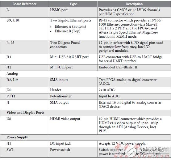
Two Gigabit Ethernet (GbE) RJ-45 ports
One mini-USB2.0 UART
One HDMI video output
One universal HSMC connector (see HSMC expansion cards)
Two 12-pin DigilentPmodTM Compatible connectors (see PmodTM Compatible expansion cards)
Analog
Two MAX 10 FPGA ADC SMA inputs
2x10 ADC header
Potentiometer input to ADC
One external 16 bit digital-to-analog converter (DAC) device with SMA output
Clocking
25 MHz single-ended, external oscillator clock source
Silicon labs clock generator with programmable frequency GUI
Switches, push buttons, jumpers, and status LEDs
Mini-USB cable for on-board USB-Blaster II
2A power supply and cord
Free Quartus® II Web Edition design software (download software and license from the website)
Complete documentation
User manual, bill of materials, schematic, and board files 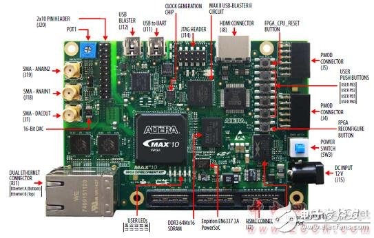
Figure 1. Distribution of major components of the Altera® MAX® 10 FPGA Development Board (front) 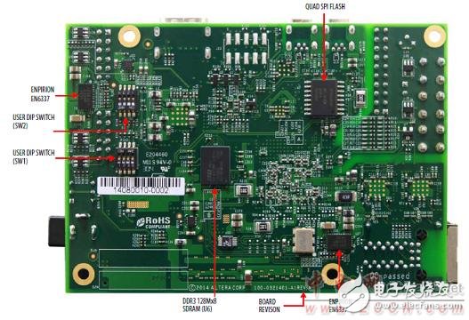
Figure 2. Main components of the Altera® MAX® 10 FPGA Development Board (back) 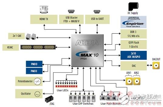
Figure 3. System Block Diagram of the Altera® MAX® 10 FPGA Development Board 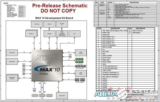
Figure 4. Circuit Diagram of Altera® MAX® 10 FPGA Development Board (1) 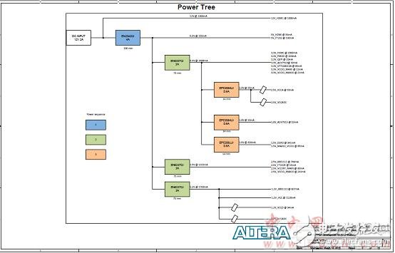
Figure 5. Circuit Diagram of Altera® MAX® 10 FPGA Development Board (2) 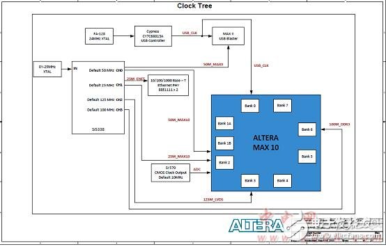
Figure 6. Circuit Diagram of Altera® MAX® 10 FPGA Development Board (3) 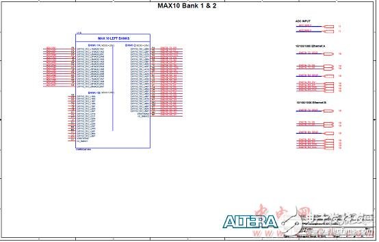
Figure 7. Circuit Diagram of Altera® MAX® 10 FPGA Development Board (4) 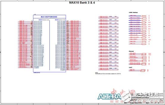
Figure 8. Circuit Diagram of Altera® MAX® 10 FPGA Development Board (5) 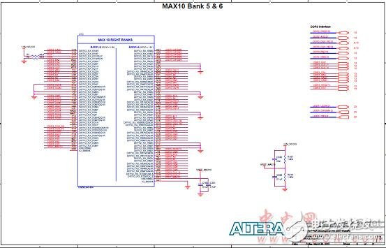
Figure 9. Circuit Diagram of Altera® MAX® 10 FPGA Development Board (6) 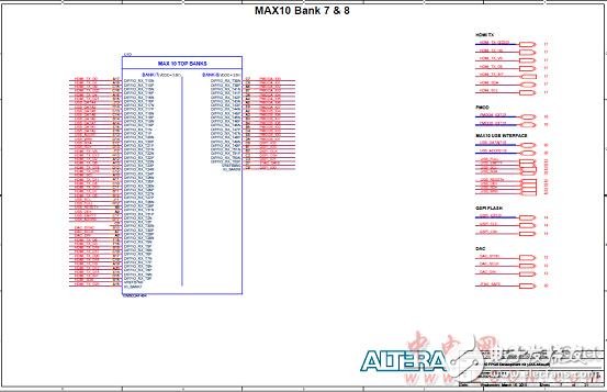
Figure 10. Altera® MAX® 10 FPGA Development Board Schematic (7) 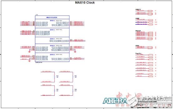
Figure 11. Circuit Diagram of Altera® MAX® 10 FPGA Development Board (8) 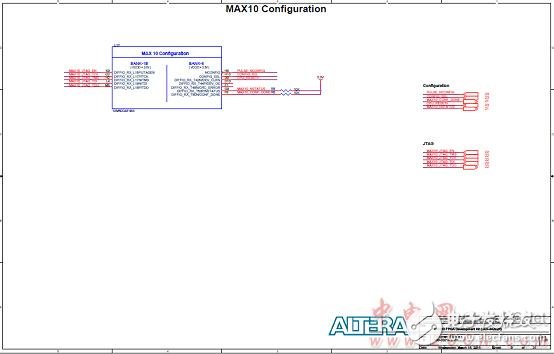
Figure 12. Circuit Diagram of the Altera® MAX® 10 FPGA Development Board (9) 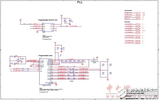
Figure 13. Circuit Diagram of Altera® MAX® 10 FPGA Development Board (10) 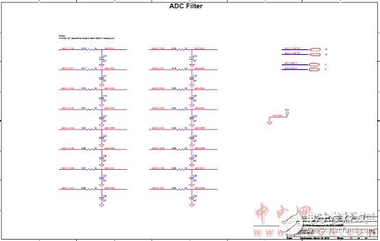
Figure 14. Circuit Diagram of Altera® MAX® 10 FPGA Development Board (11) 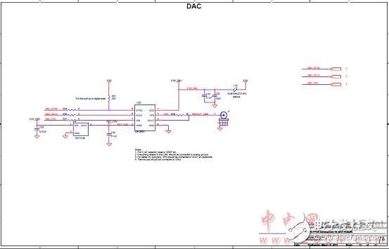
Figure 15. Circuit Diagram of Altera® MAX® 10 FPGA Development Board (12) 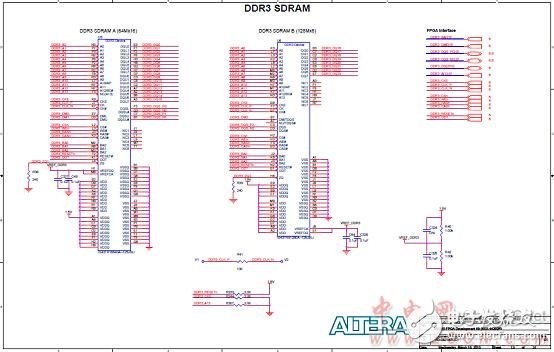
Figure 16. Altera® MAX® 10 FPGA Development Board Schematic (13) 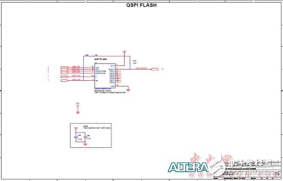
Figure 17. Altera® MAX® 10 FPGA Development Board Circuit Diagram (14) 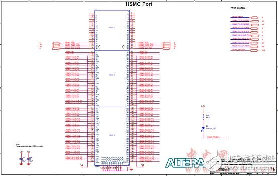
Figure 18. Circuit Diagram of Altera® MAX® 10 FPGA Development Board (15) 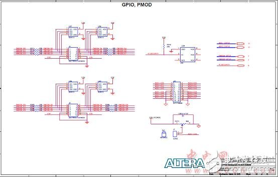
Figure 19. Circuit Diagram of Altera® MAX® 10 FPGA Development Board (16) 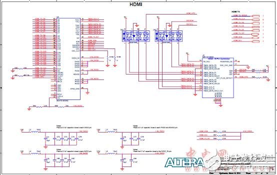
Figure 20. Circuit Diagram of Altera® MAX® 10 FPGA Development Board (17) 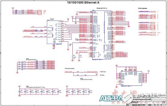
Figure 21. Circuit Diagram of Altera® MAX® 10 FPGA Development Board (18) 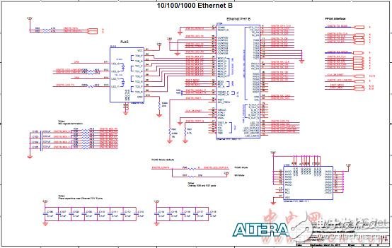
Figure 22. Circuit Diagram of Altera® MAX® 10 FPGA Development Board (19) 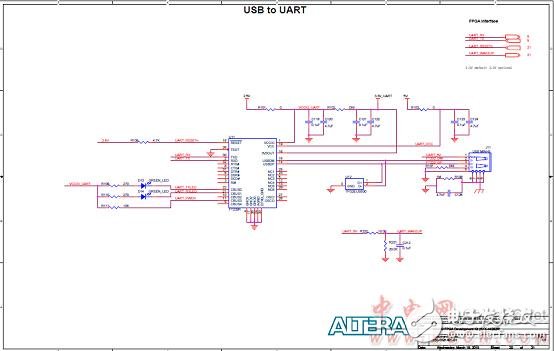
Figure 23. Circuit Diagram of Altera® MAX® 10 FPGA Development Board (20) 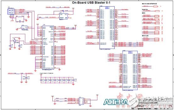
Figure 24. Circuit Diagram of Altera® MAX® 10 FPGA Development Board (21) 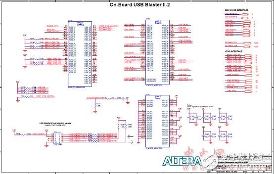
Figure 25. Circuit Diagram of Altera® MAX® 10 FPGA Development Board (22) 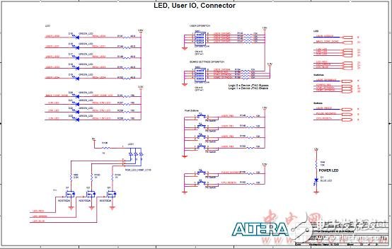
Figure 26. Circuit Diagram of Altera® MAX® 10 FPGA Development Board (23) 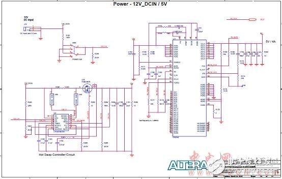
Figure 27. Circuit Diagram of Altera® MAX® 10 FPGA Development Board (24) 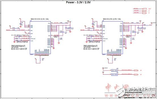
Figure 28. Altera® MAX® 10 FPGA Development Board Circuit Diagram (25) 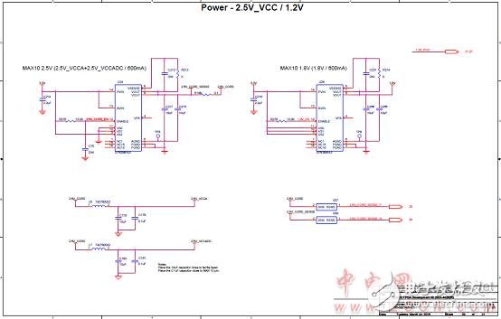
Figure 29. Altera® MAX® 10 FPGA Development Board Circuit Diagram (26) 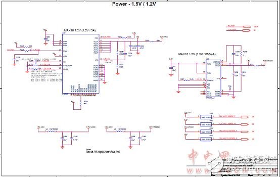
Figure 30. Circuit Diagram of the Altera® MAX® 10 FPGA Development Board (27) 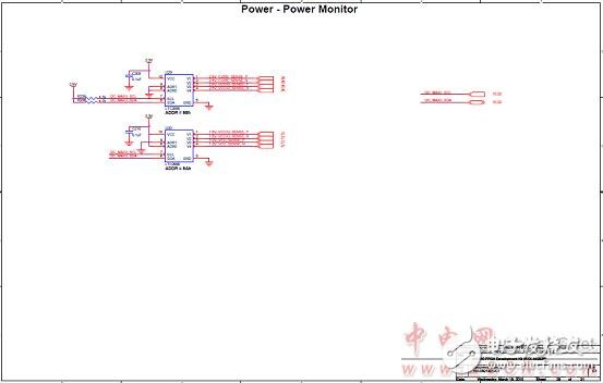
Figure 31. Circuit Diagram of Altera® MAX® 10 FPGA Development Board (28) 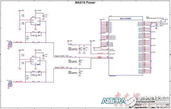
Figure 32. Circuit Diagram of Altera® MAX® 10 FPGA Development Board (29) 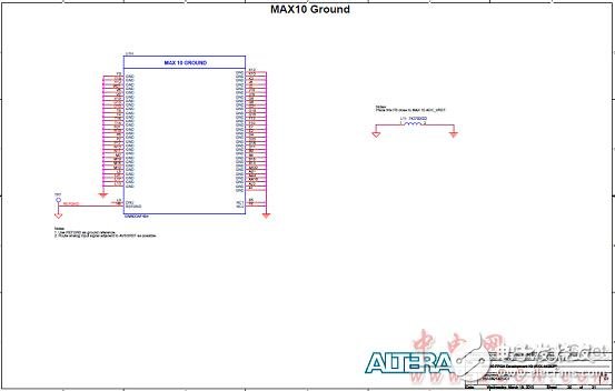
Figure 33. Circuit Diagram of the Altera® MAX® 10 FPGA Development Board (30) 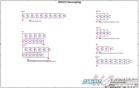
Figure 34. Circuit Diagram of the Altera® MAX® 10 FPGA Development Board (31)
MAX 10 FPGA Development Board Key Components: 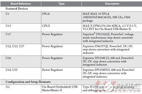
What is a fiber optic slip ring?
How do fiber optic slip rings work?
Types of fiber optic slip rings
Advantages of fiber optic slip rings
Disadvantages of fiber optic slip rings
Conclusion: What are the benefits and drawbacks of fiber optic slip rings?