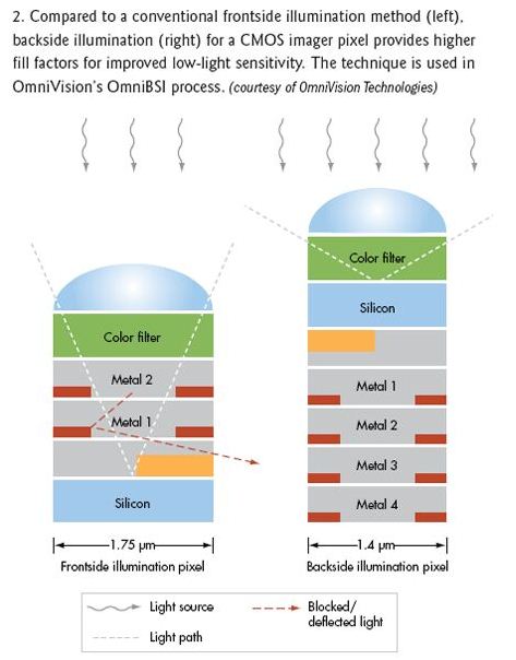
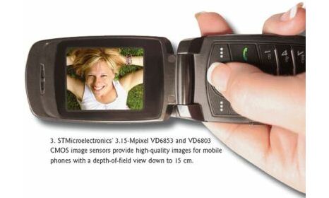
The latest generation of CMOS and CCD image sensors have greater spectral width, higher sensitivity, lower operating noise and smaller form factor. More advanced manufacturing processes also achieve lower costs. In addition, innovative architectures are bringing greater flexibility and versatility to circuit design. As a result, image sensors are now widely used in cell phones, notebooks and laptops, digital cameras, video game consoles, toys, medical devices, automobiles, security devices, industrial equipment, and many other applications. IC Insights predicts that CMOS and CCD image sensors will achieve a compound annual growth rate (CAGR) of 14% over the next five years. Both types of image sensors have found a wide range of applications, but CMOS image sensors are particularly promising. In 2012, its market share will rise from 58% last year to 73%. As with most electronic devices, performance and cost will remain a major issue for CMOS and CCD image sensors. Although CMOS image sensors are expected to have more applications, CCD image sensors are still required in applications requiring high performance. This is not a simple question of which image sensor is better. CMOS or CCD sensors are probably the best choice depending on performance and cost considerations for your specific application. CMOS image sensors are generally cheaper than CCD image sensors, so there is no doubt that CMOS image sensors can be found in many consumer electronics that emphasize low cost. Its performance has been continuously improved, and it has now entered the automotive safety application traditionally dominated by CCD image sensors, because its performance is acceptable and lower cost. CCD image sensors offer higher performance for industrial and machine vision inspection applications, as well as safety systems, scientific and military aerospace applications. They have also found applications in some niche markets, such as astronomy and medical fields. The cost of CCD image sensors is also declining, but performance is still far superior to CMOS image sensors. CMOS image sensor performance is improving CMOS image sensors are meeting many of the system requirements dictated by a variety of parameters, such as greater bandwidth and full frame shutter capability. New design and manufacturing recommendations and their implementation will drive their performance to higher. A new idea proposed by NASA's Jet Propulsion Laboratory (JPL) will effectively reduce the scattering crosstalk of image sensors. The researchers recommend adding two implants to each CMOS pixel that can affect the vertical isolation between the MOSFET and the pixel photodiode used in the imager (Figure 1). They believe that this isolation optimizes both MOSFET and photodiode performance, eliminating or significantly reducing crosstalk and noise while improving sensitivity, spatial resolution, and color fidelity. Figure 1: Compared to conventional imagers (left), the proposed CMOS imager pixel device uses deeper p and n well structures to significantly reduce crosstalk and improve overall imager sensitivity and color fidelity. Image synchronization and operation (especially in machine vision automated inspection applications) under difficult and unfavorable conditions are major challenges for CMOS image sensor designers. The industry has traditionally relied on CCD image sensors that utilize interline transfer technology to achieve high speed shutters for clear images. Recent advances in CMOS image sensors have enabled such sensors to successfully enter machine vision applications. With the advantages of parallel output, window adjustment and on-chip integration, some CMOS image sensors are now comparable to CCD image sensors used in some machine vision applications. For example, Cmosis's CMOS image sensor has a full-frame shutter function. Thanks to the ducted full-frame shutter pixel technology, this imaging system captures the next frame during data reading. Its principle is to integrate a memory node in each pixel of the image sensor, and the signal will be transmitted to this node after the image capture step is completed. Storage nodes have a particularly low parasitic light sensitivity. Each pixel is read with very low noise and a wide dynamic range. Cmosis has also developed a fast ADC that is installed in the sensor pixel column. Dalsa has also developed an interline transfer CMOS image sensor with a fast shutter function. These sensors provide the sensitivity, signal capacity, noise performance and dynamic range required for many machine vision applications. Photonfocus uses its proprietary LinLog technology in its A1312 CMOS image sensor for fast shutter speeds and wide dynamic range of up to 120dB. The sensor has a resolution of 1312 × 1028 pixels, each pixel size is 8 × 8μm, and the working speed can reach 110 frames / sec at the highest resolution. As pixel sizes of CMOS image sensors continue to shrink, it has become increasingly difficult to maintain image sensor performance and image quality. Backside illumination technology is one of the solutions. Working with TSMC, OmniVision believes it has found the secret to success with the OmniBSI approach (Figure 2). OmniVision can now produce 8 megapixel CMOS image sensors for mobile phones in a 1.4μm process. Figure 2: Backside illuminated (right) CMOS imager pixels provide a higher fill factor than conventional front exposure methods (left), thus improving sensitivity in low brightness conditions. This technology has been used in OmniVision's OmniBSI process. Sony has also succeeded in back-illumination technology. The company has produced a 5 megapixel CMOS image sensor for mobile phones, digital cameras and video cameras using the 1.75 μm process. Through cooperation with French CEA Leti and Tracit Technologies, ST has successfully demonstrated the feasibility of using a back-illumination technology to fabricate a 3 megapixel CMOS image sensor on the 1.45 process. Image quality is improving One of the more high-performance CMOS image sensors that penetrate into the consumer electronics market is ST's first 0.25-inch optical format 3.15 million-pixel CMOS image sensor. According to ST, the VD6853 and VD6803 image sensors are manufactured in a 1.75μm process and provide outstanding image quality with a focusing distance as short as 15 cm (Figure 3). Figure 3: STMicroelectronics' 3.15 megapixel VD6853 and VD6803 CMOS image sensors provide high quality images for mobile phones with depth of field as shallow as 15 cm. An embedded image enhancement filter with a four-channel inverse imaginary circuit balances uneven illumination and can be corrected for defects during imaging. These image sensors can be used in cell phones, notebook cameras, toys, and even machine vision applications. The VD683 provides a 10-bit parallel interface and the VD6803 provides a CCP2 interface. Recently, South Korea's Samsung introduced a 1.2-megapixel SoC image sensor with a 0.25-inch optical format with a maximum resolution of 1280×960 pixels. The S5K4AW CMOS image sensor for notebooks and desktops meets the special needs of high-definition real-time video applications by dividing the image into 2×2 groups, and displays images in standard VGA format without cropping. At this year's IEEE International Solid State Circuits Conference (ISSCC), Canon's 3.3 megapixel CMOS image sensor promises to deliver higher quality video and image processing capabilities for mobile devices. This high performance is achieved by using a new column read circuit that reduces noise by 30%. 3.6V Cylindrical Battery,3.6V 600Mah Ni-Cd Battery,3.6V 800Mah Ni-Mh Battery,Ni-Mh Battery 3.6V 800Mah Langrui Energy (Shenzhen) Co.,Ltd , https://www.langruibattery.com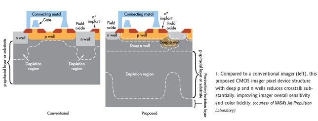
Model
Nominal Voltage
Nominal Capacity
Nominal impedance
Dimension
Charge-discharge standard
Approx Weight
(V)
(mAh)
(mQ)
Diameter
Height
Charge
Discharge
≈g
ICR10220
3.7
130
<150
10
22
0.5C-1C
0.5C-1C
4.1
ICR10440
3.7
350
<120
10
44
0.5C-1C
0.5C-1C
9
ICR14430
3.7
650
<100
13.8
42.8
0.5C-1C
0.5C-1C
17
ICR14500
3.7
900
<80
14
50
0.5C-1C
0.5C-1C
19.5
ICR17280
3.7
600
<100
16.3
28
0.5C-1C
0.5C-1C
15
ICR17335
3.7
700
<100
16.3
33.5
0.5C-1C
0.5C-1C
18
ICR18500
3.7
1400
<70
18.1
50
0.5C-1C
0.5C-1C
33
ICR18650
3.7
2000
<50
18.1
64.8
0.5C-1C
0.5C-1C
45
ICR18650P
3.7
2000
<40
18.1
65
0.5C-1C
3C-5C
45
ICR18650P
3.7
2200
<40
18.1
65
0.5C-1C
3C-5C
45
ICR18650
3.7
2600
<70
18.1
64.8
0.5C-1C
0.5C-1C
45
ICR26650
3.7
3500
<30
26
65.5
0.5C-1C
0.5C-1C
85
ICR26650P
3.7
5000
<30
26
65.5
0.5C-1C
0.5C-1C
85
ICR18650P
3.7
1500
<15
18.1
64.8
1C
10C-15C
47
ICR26650P
3.7
2200
<15
26
64.8
1C
10C-15C
64
IFR14430E
3.2
400
<115
13.8
43
0.5C-1C
0.5C-1C
15
IFR14500E
3.2
400
<95
13.8
50.2
0.5C-1C
0.5C-1C
15.5
IFR14500E
3.2
650
<80
13.8
50.2
0.5C-1C
0.5C-1C
17.8
IFR18500E
3.2
600
<80
18
50
0.5C-1C
0.5C-1C
19.5
IFR18500E
3.2
1200
<80
18
64.8
0.5C-1C
0.5C-1C
30.4
IFR18650E
3.2
1500
<65
18
64.8
0.5C-1C
0.5C-1C
40.5
IFR18650E
3.2
1700
<80
18
65.3
0.5C-1C
0.5C-1C
41.2
IFR26650E
3.2
3400
<20
26
65.3
0.5C-1C
0.5C-1C
87
IFR18650P
3.2
1100
<20
18
65.3
1-3C
10-25C
40
IFR26650P
3.2
2400
<20
26
65.3
1-3C
10-25C
82