Abstract: SAA7110 is a programmable front-end video decoder produced by Philips, which can convert input video signals into YUV digital signals. The article introduces the main characteristics, structural principles and pin functions of SAA7110, compares the differences between SAA7110 and SAA7110, gives the important pins that should be paid attention to in the application, and finally introduces its application connection and an image acquisition system. Application structure. The video decoder SAA710 is a programmable front-end video decoder produced by Philips. Compared with SAA7111, although some of the pin signals are similar, there is still a big difference, which needs to be given enough attention in practical applications. Most of the domestic video capture or image capture use SAA7111, and the SAA7110 mentioned more often did not see much information to discuss it in detail. In product production, only a few domestic companies (such as Beijing Jiaheng Zhongzi Image Technology Co., Ltd.) use the chip. Based on scientific research and practical needs, this article makes a detailed discussion on the main features, structural functions, and pin applications of SAA710. The main features of SAA710 are as follows: ◠With 6 analog inputs (4 × CVBS, 3 × Y / C or a combination of both); ◠With 3 analog processing channels; ◠Built-in 3-way anti-aliasing filter; ◠Can add 2 channel analog signals; ◠Contains 2 8-bit CMOS video A / D converters; ◠Programmable static gain control or automatic gain control for the selected CVBS / Y channel; ◠Can control the white peak; ◠Can process brightness and chroma of PALB / G, NTSC M, SECAM system; ◠Automatically perform 50 / 60Hz field frequency detection and automatic conversion between standard PAL and NTSC, forced SECAM; ◠Line and field synchronization detection can be realized for all systems; ◠For the PA system, the delay line of the UV signal can be used to correct the phase difference of the chrominance signal; ◠YUV bus supports the following data rates: —780 × fh = 12.2727MHz, 60Hz (NTSC); -944 × fh = 14.75MHz, 50Hz (PAL / SECAM); ◠The data output format has two types: YUV 4: 1: 1 (8bit) and YUV 4: 2: 2 (8bit); ◠User programmable for peak brightness aperture correction; ◠All systems can use the same frequency circuit crystal oscillator (26.8MHz); ◠With real-time status information output (RTCO); ◠The output pin has a user programmable universal switch; ◠On-chip conversion between the clock generation circuit (CGC) and external CGC (SAA7197); ◠With power-on control function; ◠With controllable I2C bus; ◠Compatible with CCIR601 standard. 2.1 Structural principle The functional block diagram of SAA710 is shown in Figure 1. The main part of the block diagram will be described below. (1) Analog input processing SAA710 has six analog signal inputs, and the two analog main channels are composed of clamping circuit, analog amplifier, anti-aliasing filter, and video CMOS A / D converter. The other analog channel also contains a clamping circuit, analog amplifier, and anti-aliasing filter, and can be added to or directly converted to the two main channels before A / D conversion. The clamping control circuit controls the correct clamping of the analog input signal. High frequency coupling capacitors are used to store and filter the clamping voltage. For luminance or CVBS signals, the usual digital clamping standard is 64, while the chrominance signal is 128. The gain control circuit generates the static gain standard of three analog amplifiers through the bus, and one of them can also be controlled by the built-in automatic gain control (AGC) circuit. The role of AGC is to amplify the CVBS or Y signal to the desired signal amplitude so that it is the same as the ADC input voltage range. The anti-aliasing filter should be suitable for the clock frequency. The vertical blanking control circuit is used to generate bus programmable vertical blanking pulses. During the vertical blanking period, gain and clamp control are invalid. (3) Chromaticity circuit After the 8-bit digital chrominance signal passes through the input interface, it can pass the chrominance band-pass filter to reduce the DC component, and then sent to the multiplication input of the quadrature demodulator. In the two subcarrier signals from the local oscillator DTO1 (discrete time oscillator), the phase shift of the subcarrier signal is 90 °, and the frequency is determined by the color system of the currently input video signal. For all PAL and NTSC signals, the multiplier can be used as a quadrature demodulator; for SECAM signals, the multiplier can be used as a down-converter. After the two multiplied output signals are converted into a continuous stream of UV data, they can be used in two low-pass filter stages and then added to a gain-controlled amplifier. The last multiplexed low-pass filter will be used with the previous stage to set the required bandwidth. The original signals of PAL and NTSC flow into the comb filter. The SECAM original signal is fed through a bell filter (center frequency is 0 Hz), phase demodulator and differentiator to obtain frequency-demodulated color-difference signals. De-emphasize the SECAM signal and feed it to the cross-conversion, which can produce continuous transmission of color difference signals. After these signals are sent to BCS (brightness, contrast, saturation) for processing, they will finally reach the output format level and output interface. Figure 2 shows the working process diagram of the chroma circuit. (4) Brightness circuit The 8-bit brightness signal (digital CVBS format or brightness format (S-VHS, HI8)) is fed through a convertible pre-filter. The enhancement of high frequency components can make up for the loss. The chroma notch filter (fc = 4.43 MHz or 3.58 MHz, center frequency is optional) can eliminate most color carrier signals, so the S-Video (S-VHS, HI8) signal must pass normally. The high-frequency component of the luminance signal can be enhanced in two band-pass filters with selectable transmission properties (sharpness increase is controlled via the I2C bus). And can enhance the signal once again in the optional core circuit, and then add the signal to the original (non-elevated) signal. The enhanced brightness signal is fed to the BCS control and output interface through variable delay. (5) Digital YUV bus Through the 16bitYUV bus, digital information can be transferred from the output interface to the field storage, digital color space converter (SAA7192 DCSC) or video enhanced analog-to-digital processor (SAA7165 VEDA2). These outputs can be controlled by FEIN. YUV data rate is equal to LLC2. The output signals Y7 ~ Y0 are bit bits of the digital brightness signal. The output signals UV7 to UV0 are bit bits of the multiplexed color difference signals (B to Y) and (R to Y). The time frame in the format table is the time required to transmit a complete sample. The time frame can be controlled by the HREF signal. The fast enable can be obtained by setting FEIN low. This signal can also be used to control the rapid switching of the digital YAV bus. When the FEIN pin is high, it will force the Y and UV outputs to a high impedance state. (6) Synchronous processing After the pre-filtered brightness signal is sent to the synchronization stage. The sync pulses are sent to the phase detector after being split, where they are compared with the subdivided clock frequency, and the results are output to the loop filter to store all the phase difference information. The adjustable output signals HCL and HSY are generated by the requirements of the analog front end. The output signals HS, VS, and PLIN are locked to the time reference mark to ensure that they are located between the input signal and the HREF signal. This is because further improvements in the circuit may change the overall processing delay, so it is not recommended to use it for input Where the timing of the signal requires absolute accuracy. Driving an oscillator with a loop filter can generate the line frequency control signal LFCO. 2.2 Pin function Figure 3 shows the pinout diagram of SAA710. The functions of the main pins are as follows: SP: Test input pin, this pin should be grounded during normal operation. AP: Test input pin. When the (action pin) is in normal operation, this pin should also be grounded. RTCO: Real-time control output. This pin is used to match the increment of HPLL, FSC-PLL and the sequence information of PAL or SECAM. SDA: I2C bus serial data input / output. SCL: I2C bus serial clock input. VDD, VSS: respectively + 5V power supply and ground terminal. AIXX: analog input pin. AOUT: Analog output pin. LFCO: horizontal frequency control output pin; the analog clock signal can be used to drive an external CGC; its frequency is a multiple of the actual horizontal frequency (7.375 / 6.1336MHz). LLC: line lock clock input / output pin. When CGCE is 1, the pin is output; when CGCE is 0, the pin is input). LLC2: line-locked clock divided by 2 input and output; FLLC2 = 0.5fLLC. When CGCE is 1, this pin is output; when CGCE is 0, this pin is in high impedance state). CREF: Reference clock input / output pin (output when CGCE = 1; input when CGCE = 0). RESET: Reset signal, low level is effective. CGCE: CGC enable input pin. When CGCE is 1, it is valid in the chip CGC; when CGCE is 0, the external CGC mode is used and SAA7197 can be used. HCL: horizontal clamp input / output pulse, which can be programmed through the I2C bus PULIO bit: output when PULIO is 1; input when PULIO is 0. This signal can be used to indicate the high-level clamping time for the analog input interface. The start and end of the high level can be controlled by programming the I2C bus register (only in output mode). HSY: horizontal synchronous input / output, which can be programmed through the PULIO bit of the I2C bus: PULIO is output when 1; PULIO is input when 0 This signal can be sent to the analog interface. The start and end of the high level can be controlled by programming the I2C bus register (only in output mode). HS: horizontal synchronization output. Its positive slope position is programmable. PLIN (HL): The PAL does not output the identification pin. The demodulated PAL signal can send a line feed signal (PLIN = 0) or a non-line feed signal (PLIN = 1). After demodulating SECAM, it can send a DR line signal (PLIN = 0) or DB line signal (PLIN = 1). The PLIN function can be selected by setting the RTSE of the I2C bus to 0 (H-PLL output lock; a high level indicates that the internal PLC has been locked); and the HL function can be selected by setting the RTSE of the I2C bus to 1. ODD (VL): Odd and even field output indicator, high level means odd field. The ODD function can be selected by setting the RTSE of the I2C bus to 0 (vertical output lock; high level indicates that the internal VNL (vertical noise limiter) is in the locked state); the VL function can be selected by setting the RTSE of the I2C bus to 1. VS: Vertical synchronous input / output (programmable through the OEHV bit of the I2C bus: OEHV is output when 1; OEHV is input when 0). This signal can be used to indicate vertical synchronization with YUV output. At VNL, its high level period is close to 6 lines. The positive slope includes the phase information of the deflection controller (such as TDA9150). In input mode, this signal is used to synchronize vertical gain and clamp blanking, and is active high. HREF: horizontal reference output, this signal indicates that there is data on the digital YUV bus. A positive slope indicates the start of a new scan line. Whether the high level of HREF is 768 Y sampling points or 640 Y sampling points depends on the field frequency (50/60 Hz). In addition, HREF can also be used to synchronize data multiplexers or demultiplexers. During the vertical blanking signal, HREF also exists. Y7 ~ Y0: 8-bit brightness (Y) digital output. By setting the SQPB of the I2C bus to be a part of the 1 selectable digital YUV bus (data rate LLC / 2), or A / D2 (3) output (data rate LLC / 2). UV7 ~ UV0: 8-bit digital UV (color difference) output, used to output the multiplexed color difference signal of the UV component after demodulation of the CVBS signal or chrominance signal. The format and multiplex mode can be selected and controlled through the I2C bus. These signals can be selected as part of the digital YUV bus (data rate LLC / 2) or A / D2 (3) output (data rate LLC / 2) by setting the SQPB of the I2C bus to 1. FEIN (MUXC): Quick input enable signal (active low), which can be used to control the rapid switching of the digital YUV bus. Input high level can make the Y and UV output of the film become high impedance. To use this function, the MS24, MS34, and MUYC of the bus must be set low (respectively for the multiplexed component input; the control signal of the analog multiplexer that locks the Y / C signal and the CVBS signal quickly). If one of MS24, MS34, MUYC is high level, then FEIN will be automatically set low (digital YUV bus is valid). GPSSW (VBLK): general-purpose switch output, this signal can be programmed by bit 1 of 0DH of I2C bus. By setting VBLKA of the I2C bus to 0, the GPS function (vertical blanking test output) can be selected. XTAL0: crystal oscillator output (to 26.8MHz crystal oscillator); it is not necessary when using TTL clock. XTAL1: crystal oscillator input (26.8MHz crystal oscillator) or connect an external clock compatible with TTL square wave clock signal. 3 Application 3.1 Typical applications Fig. 4 is the typical application connection circuit of SAA710. As long as a video signal is input to the input of SAA710 in this circuit, digital signals of different formats can be obtained at the output. This circuit has important applications in the analog-to-digital conversion of video processing. 3.2 PCI bus high-speed video image acquisition card The PCI bus is a high-performance local bus. It supports 32-bit / 64-bit data transmission and linear burst mode with a transmission rate of up to 133 Mbps. It also supports plug-and-play and is very suitable for the design needs of image acquisition cards. In addition, the use of the PCI bus port provided by the SAA7146 desktop multimedia application chip produced by Philips can also support PC video applications (see related materials). Figure 5 is a functional block diagram of a high-speed video image acquisition system based on PCI bus. SAA7110 and SAA7146 are the main part of the frame grabber, which can realize high-speed data transmission with PC through PCI local bus. Here, SAA710 mainly completes the sampling, quantization and decoding of analog video signals. The main pins of SAA7146 used in the hardware design of this capture card are VS-A, VS-B, HS-A, HS-B, pxq-A, pxq-B, LLC-A, LLC-B, GPIO3∽0 Wait. At the same time, in the PCB wiring, SAA7146 should be as close as possible to the PCI socket to ensure normal operation. The main problems involved in the software driver design are: using PCI BIOS to obtain the PCI configuration parameters of the acquisition card, applying for RPS physical space and image physical space, register assignment of SAA 7146 and SAA 7110 initialization, writing SAA 7146 acquisition image RPS interrupt service program Driver and application interface, etc. The author has used DDD to develop drivers under WIN98 to collect images. The actual use proves that the collected images have a higher resolution and the images are very clear, which can meet the actual needs. Follow WeChat Download Audiophile APP Follow the audiophile class related suggestion In order to realize the intelligent analysis function of high-definition video, this article introduces a high-definition video intelligent analysis system based on TI's DM8168 ... The characteristics of the digital video codec technology field are a wide variety, coexistence of multiple types, coexistence of old and new, and rapid development of research and development. There is no digital video of that kind ... As early as 2008, high-definition video surveillance has been proposed by the industry and once became a hot spot of concern, but due to the technology, cost and actual customer needs at that time ... Da Vinci technology is a new platform for digital image, video, voice, and audio signal processing. Once launched, it is warmly welcomed. Based on it ... The demand for digital video products has skyrocketed in recent years. Mainstream applications include video communications, video surveillance and industrial automation, and the most popular applications are entertainment applications, ... With the development of TV technology to digitalization, many digital devices have also appeared in the TV monitoring industry, and digital systems have become the current hot spot, so ... The design and implementation of a new type of aircraft airborne digital video recorder introduces a method and number of aircraft video recording using digital technology ... Discussion on the basic knowledge of digital video Due to the needs of the work, I have done several years of development in digital video processing. The development I mean refers to the application layer ... The basic classification of digital video recorders (DVR) DVR In the early stage of development, due to the controversy and variety of DVRs, many people in the industry have "... 1. Foreword-Digital TV has entered without knowing ... Abstract: Introduces the development background and technical advantages of the new digital video interface, and analyzes the communication protocol of DVI 1.0 and T. M. D. S ... '+ data.data.username +' '; dom + =' Guangzhou Ehang Electronic Co., Ltd. , https://www.ehangmobile.com
1 Main features 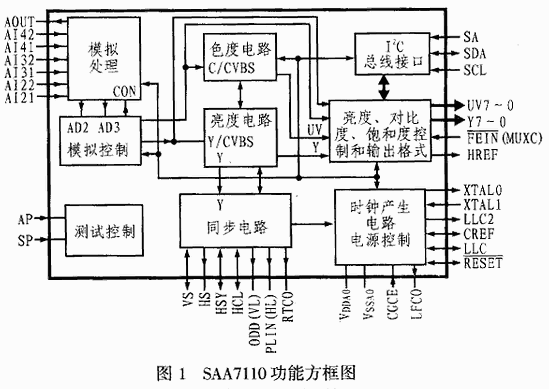
â— It can be controlled by the whole HUE;
figure 2
â— Brightness, contrast and saturation (BCS) control can be performed on the YUV bus;
2 Structure principle and pin function 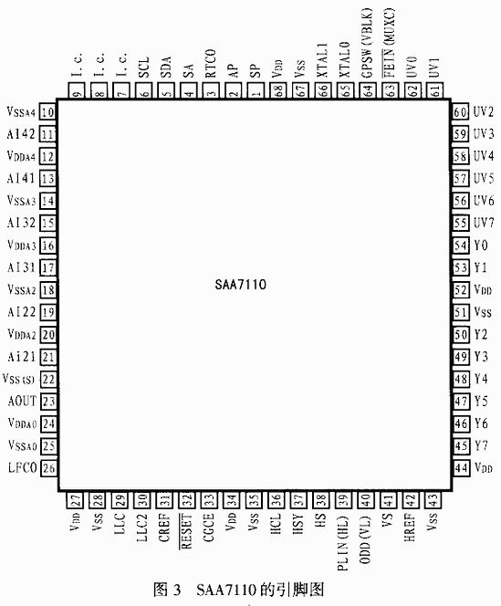
(2) Analog control circuit
Figure 4
SA: I2C bus slave address selection input. At low level, if the slave address is 9CH, then write; if the slave address is 9DH, then read. While at high level, the slave address is written when it is 9DH and read when it is 9FH. 


'+ data.username +'
'+ data.username +'
'; dom + ='
'; $ (' # follow_list '). append (follow_user);} if (data.status == "failed") {alert (data.msg);}});} else {// Unfollow if ($ ( this) .attr ('id') == 'cancelFollow') {$ .post ('/ d / user / cancelFollow', {tuid: article_user_id}, function (data) {// Data format returned: if (data .status == "successed") {follow_wrap.html ('Follow'). attr ('id', 'follow'). css ('background', '# f90'); $ (". followNum strong"). html (-getFollowNum); $ ('# follow_list .face'). each (function () {var target_uid = $ (this) .attr ('data-uid'); if (target_uid == now_uid) {$ ( this) .remove ();}})} if (data.status == "failed") {alert (data.msg);}}); return false;}}});});}); / * var myface = "{$ _super ['uid'] | avatar}"; var myname = "{$ _super ['username']}"; var article_id = {$ article ['id']}; var article_user_id = {$ article ['mid']}; // Article author ID $ (function () {<notempty name = "clearnum"> // Reduce the number of reminders var count = parseInt ($ ("# noticeCount"). html ()); count = count-{$ clearnum}; $ ("# noticeCount"). html (count); if ( count
Digital video decoder SAA7110
Interesting and informative information and technical dry goods
Create your own personal electronic circle
Lock the latest course activities and technical live broadcast
comment
Publish
Design scheme of video intelligent analysis system based on DM8168
Posted at 2014-01-10 15:44 • 3032 views
Review and Prospect of Digital Video Codec Technology
Posted at 2013-04-03 09:39 • 384 views
Megapixel camera chip technology analysis
Posted at 2012-10-08 14:43 • 938 times read
Da Vinci technical interpretation
Posted at 2012-07-11 13:50 • 485 times read
Several strategies for optimization of video algorithm system based on DSP
Posted at 2012-05-18 11:42 • 330 views
Digital video matrix technology principle and application advantages
Posted at 2010-12-17 11:24 • 378 times read
Design and Implementation of a New Type Aircraft Digital Video Recorder
Posted at 2009-12-19 10:16 • 435 views
Discussion on the basic knowledge of digital video
Published on 2009-12-18 09:34 • 286 times read
The basic classification of digital video recorder (DVR)
Published on 2008-12-29 11:29 • 263 times read
Digital Video Broadcasting (DVB)
Posted at 2006-04-17 19:10 • 241 views
Digital video interface-DVI 1.0
Published on 2006-03-24 13:29 • 1317 times read