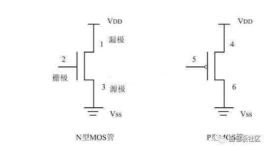
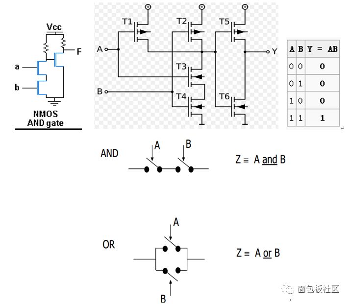
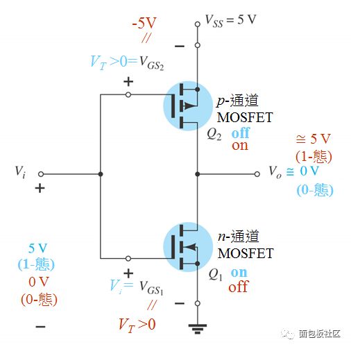
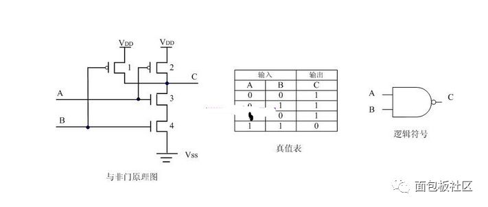
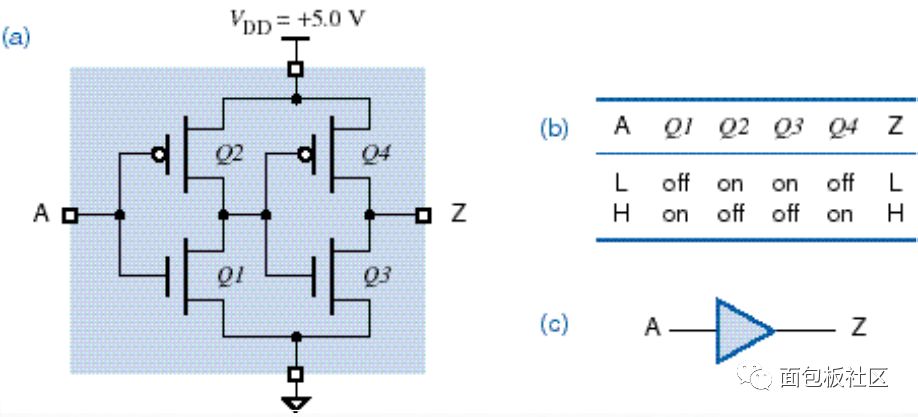
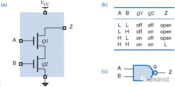
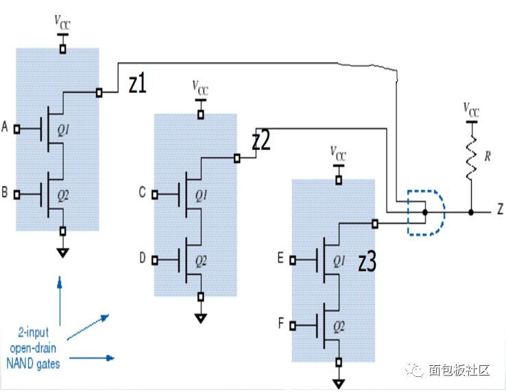
What can you get in this article? MOSFET buffer Buffer and open-drain OD gates are very important concepts of digital circuits. How to use inverters, lines, and logic? According to the schematic diagram, the truth table, the application of typical circuits to fully understand the basic logic gates, AND gates, OR gates, and NAND gates. What is the semiconductor SS, TT, FF? 1. MOS logic circuits (AND gates, OR gates, NOT gates, etc.) as Hardware engineers, can not understand the chip; but to understand the chip, MOS tube composed of a variety of basic logic circuits must be memorized in order to be able to Skillfully understand the block diagram of the chip. Field-Effect Transistors can form a variety of gate circuits through different combinations. As mentioned at the outset, these most basic unit circuits may be the basis of modern ICs. The following circuit forms exist in a large number of commonly used 74 series chips. The OD gates described later, the buffers are commonly used in the design of the GPIO port of the chip. MOS tube constitutes the basic AND gate, OR gate and gate can be composed of six tubes, through the schematic should be able to more clearly see the schematic diagram of the AND gate, and then from the truth table can see the corresponding relationship between the input and output. The corresponding circuit of the AND gate is given in this article. If you are interested, you can think about the circuit structure of the OR gate. In fact, there is a corresponding relationship between the two. 2. Inverter The following figure shows the circuit diagram of the inverter. The state of the input and output is the opposite and the inverter is called. Circuit analysis: When the input Vi is low, the upper tube is turned on, the lower tube is turned off, and the output is high. When the input Vi is high, the upper tube is turned off, the lower tube is turned on, and the output is low level. The NAND gate diagram shows the circuit diagram of the NAND gate. The NAND gate is equal to zero and the difference is one. When A, B input is low, 1,2 tube conduction, 3,4 tube cut-off, C terminal voltage and Vdd consistent, output high. When A input high level, B input low level, 1, 3 tube conduction, 2, 4 tube cut-off, C terminal potential is consistent with the drain of 1 tube, the output is high. When A is input low level, B input is high level, 2, 4 is turned on, 1, 3 tubes are cut off, C terminal potential is consistent with the drain of 2 tubes, and the output is high level. When the A and B inputs are all high, the 1 and 2 tubes are turned off, and the 3 and 4 tubes are turned on. The C terminal voltage is the same as the ground and the output is low. 4. Buffer CMOS Buffer (buffer), the buffer is opposite to the inverter, the buffer input and output are the same, the inverter input and output are the opposite. Circuit analysis: In the previous stage, Q1 and Q2 form an inverter; the following stages Q3 and Q4 form an inverter, which is equivalent to reversing the two phases, and then restored. 5. Open drain gate Open drain gate is a very classic circuit commonly used in the design of the master chip GPIO port or microcontroller GPIO port. The most important point is: Open-drain is a high-impedance state, the general application needs to be connected to a pull-up resistor. [Open drain gate application - line and logic] Z=z1z2z3 "Line AND" logic is because the transistors of the outputs of multiple logic units share a pull-up resistor. As long as one logic unit outputs a low level, that is, the open collector output (tube) is turned on, the output is low And only when all units are turned off, the output is pulled high by the pull-up resistor. This is a very practical circuit that can be used in logic arbitration and other circuit systems. Perhaps after a few years of work, the diode-transistor circuit is generally considered to be very simple, which can only indicate that the research is not enough. Sometimes things that are simpler are more complex. For example, from a process point of view, the transistor is divided into TT, SS, FF, IC design is not to bypass these, the foundation is not easy, considering more in-depth, and that only learn fur. Wire Harness,wiring,wiring harness,jamma wiring harness Guangzhou Ruihong Electronic Technology CO.,Ltd , https://www.callegame.com