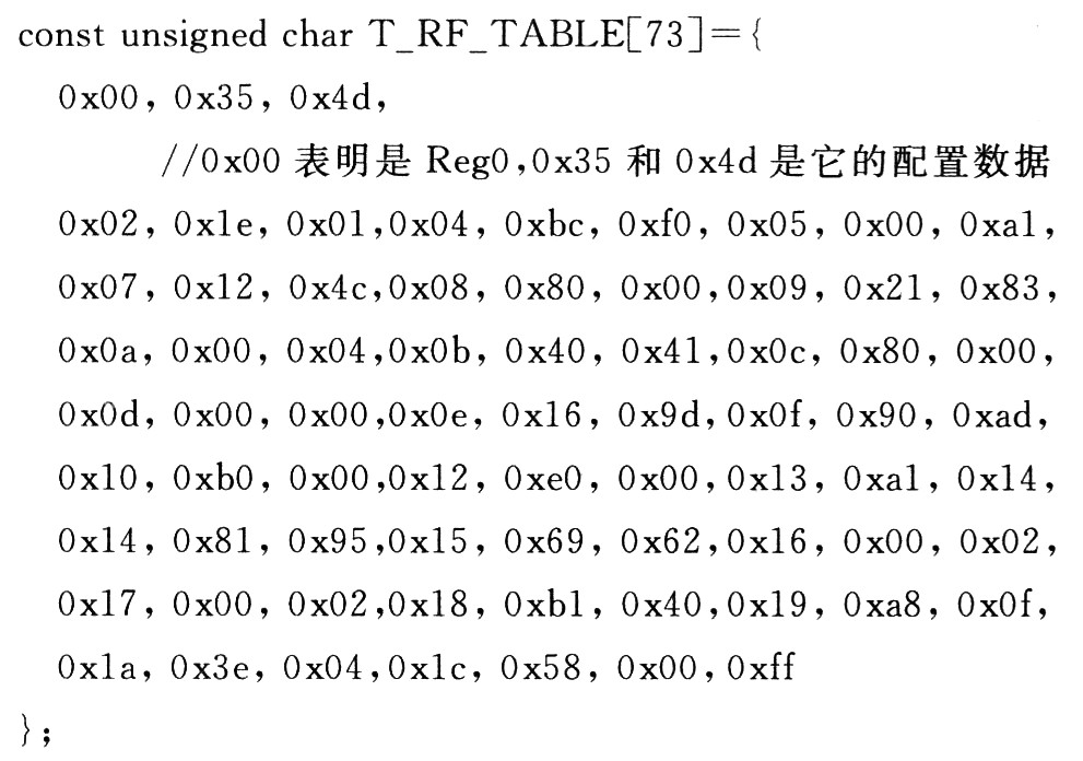
Reg0 ~ 28 is mainly to configure the transmission power, VCO, RSSI, reception delay, channel selection and control, AMS test and control, BPF and AGC control, transmission and reception data control, DC drift control, PLL synchronization control, data transmission and reception timing Control, N / VCO parameter control, clock, etc. The detailed configuration data of Reg0 ~ 28 are as follows: 18650 2S6P 7.4V Battery Pack,Rechargeable Aa Batteries,Portable Battery Charger,External Battery Pack Shenzhen Powercom Electronics Co., Ltd. , https://www.expowercome.com
1 System Overview At present, there are many integrated radio frequency chips in the 2.4 GHz frequency band, with different performances. Table 1 lists the performance characteristics of several commonly used chips. 
This system uses MSP430F247 single-chip microcomputer and EMC's EMl98810 chip to design. The MSP430 series MCU is a 16-bit reduced instruction set (RISC) microprocessor. It has a wealth of addressing methods (7 source operand addressing, 4 destination operand addressing), concise 27 core instructions and a large number of analog instructions; a large number of registers and on-chip data memory can participate in a variety of Operation; with efficient table look-up processing instructions; with high processing speed, the instruction cycle is 125 ns under the drive of 8 MHz crystal oscillator; there are many interrupt sources and can be nested arbitrarily; when the system is in a power-saving standby state, It only takes 6 μs to wake up with an interrupt request. The power supply Voltage of MSP430 series single-chip microcomputer is 1.8 ~ 3.6 V. When it runs under the clock condition of 1 MHz, the current of the chip is about 200 ~ 400μA, and the minimum clock shutdown mode is only O. 1 μA.
The EMl98810 chip has a built-in 2.4 GHz GFSK RF transceiver, with 8-bit data frame wireless transceiver function, the leading area can be set to 1-8 bytes, supports 1 to 4 word addresses (up to 64 bits), the maximum The data transmission rate is 1 Mbps, allowing long data packets to be transmitted; the frequency range is 2 400 ~ 2 482 MHz (81 channels), the transmission distance is 100 m (PCB antenna), the RF output power is 2 dBm, and the receiving sensitivity is above -85 dBm, Using SPI digital programming interface, the interface voltage is 2.5 ~ 3.7 V. The transmission power of the chip can be adjusted by digital programming, and the low power consumption mode can be easily realized through the setting of the register; built-in multiple error correction functions, using various payload data formats to eliminate DC drift; support FEC 1/3, 2/3 error correction function and CRC16 error detection function. There are two working modes of FIFO and DIRECT inside: FIFO mode is simple and easy to use, the requirements for MCU are not high, the transmission and reception each have a 64-byte buffer, and a maximum of 64 bytes of data can be processed in one transmission and reception; The requirements are higher, and the MCU needs to handle various error correction and detection functions.
2 System design
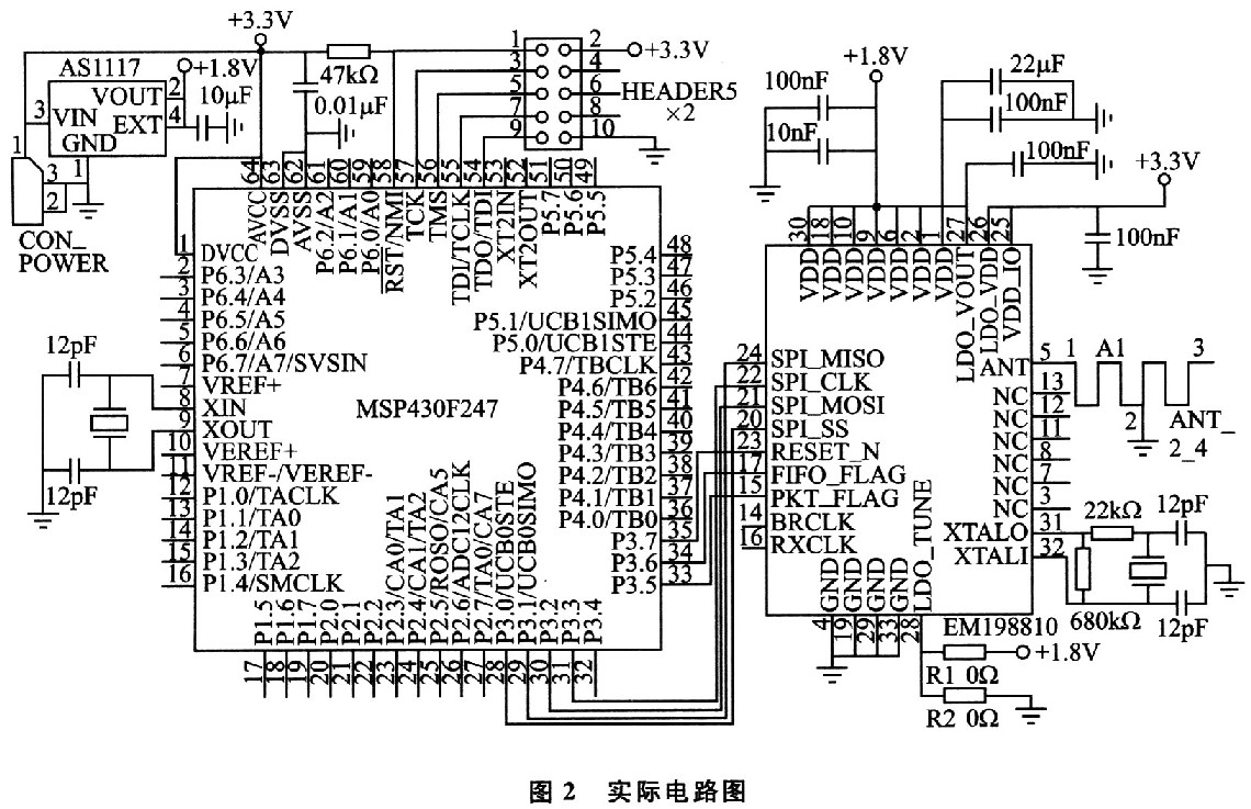
2. 1 systematic hardware design Fig. 1 is the connection schematic diagram of MSP430F247 one-chip computer and EMl98810, connect with RF chip through SPI bus line. The actual circuit connection is shown in Figure 2. 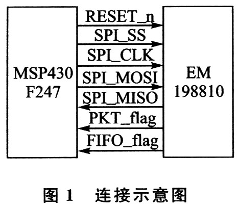
2.2 System software design The data packet format is as follows: ![]()
Among them, the leading zone can be configured from 1 to 8 bytes, the sync word can be configured to 16, 32, 48 or 64 bits; the leading tail zone can be configured to 4, 6, 8 ... 18 bits; the data zone can be NRZ code, Manch-ester code, 8/10 bit code, data with FEC 4 formats.
After the system is powered on, first make the RESET_n pin of the EMl98810 low to ensure the chip is effectively reset; then make this pin high, the BRCLK pin will generate a 12 MHz clock; and then initialize the relevant registers. The initialization procedure flow is shown in Figure 3. 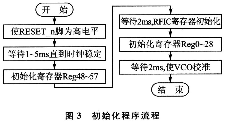
Among them, Reg48 is the data frame format configuration register, you need to set the length of the leading area (default is 3 bytes), the default sync word length is 64 bits, the leading tail length is 4 bits, and the data default is NRZ format. The second bit of this register is 1 to configure sleep mode, and the third bit is 1 to configure standby mode. Reg49 ~ 51 are used to set the delay time of transmission and reception. Reg52 ~ 55 are used to set the synchronous control word, the default is all 0000H. Reg57 is used to configure whether to enable CRC check and packet length control mode. The detailed configuration data of Reg48 ~ 57 are as follows: 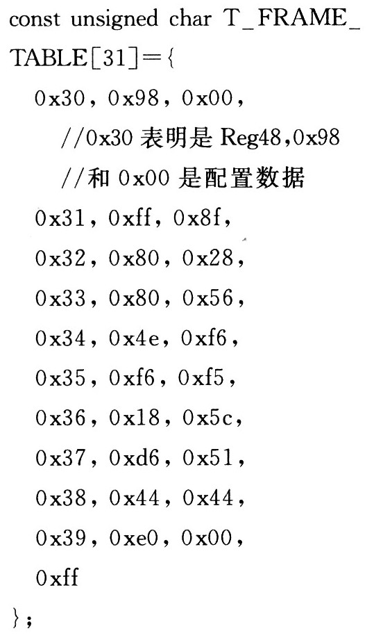
After Reg0 ~ 28 is initialized and then delayed by 2 ms, you can directly send and receive data. In particular, the frame registers Reg48-57 must be initialized before the RFIC registers Reg0-28. All registers read and write and send and receive data are carried out through the SPI interface, and only supports the slave mode, SPI operation timing is shown in Figure 4. When the 28th pin of the chip LDO_TUNE is grounded (R1 is disconnected, R2 is connected to the O Ω resistor), its data is valid at the rising edge of the SPI_CLK clock; when LDO_TUNE is connected to VDD (R2 is disconnected, R1 is connected to the 0 Ω resistor), the data is at SPI_CLK The falling edge of the clock is valid. As long as SPI_SS is high, the data in the register will remain unchanged; only when SPI_SS is low, the contents of the register can be rewritten. 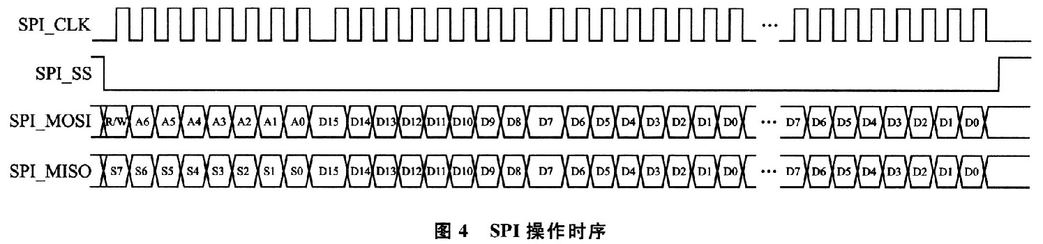
EMl98810 has two methods to detect the length of the data packet sent and received: one is automatically detected in the data frame, the maximum frame length cannot exceed 255 bytes. First set the 13th bit of Reg57 to 1, then the first byte in the send or receive data area represents the length of the data, the frame controller will automatically control the start and stop of sending and receiving. The other is to keep the state of transmission or reception unchanged, and control the correct transmission and reception of data packets through external MSP430F247.
The flow of sending data is shown in Figure 5. When transmitting data, first set the 8th bit of Reg7 to 1, allowing to enter the data transmission state under the control of the internal state machine, and then set the O ~ 6 bits of Reg7 as the selected channel. Before sending the leading and trailing data, MSP430F247 must put the data in the FIFO. If the data length exceeds 63 bytes, it should be written multiple times. FIFO_flag = 1 indicates that the FIFO is empty. MSP430F247 uses this signal as an interrupt request to ensure the real-time nature of sending data to FIF0. After the data is sent, PKT_flag = 1. 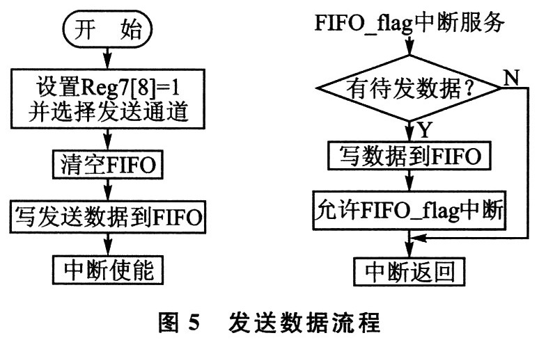
If Reg7 [7] = 1 and Reg7 [0 ~ 6] are set to the same channel as the transmission, the chip enters the automatic receiving state, and the receiving data flow is shown in Figure 6. When the sync word is detected, it will automatically receive and decode the data packet, and enter the standby mode after the reception is completed. If the received data exceeds 63 bytes, FIFO_flag = 1, MSP430F247 uses this signal as an interrupt request to ensure the real-time nature of the read data. 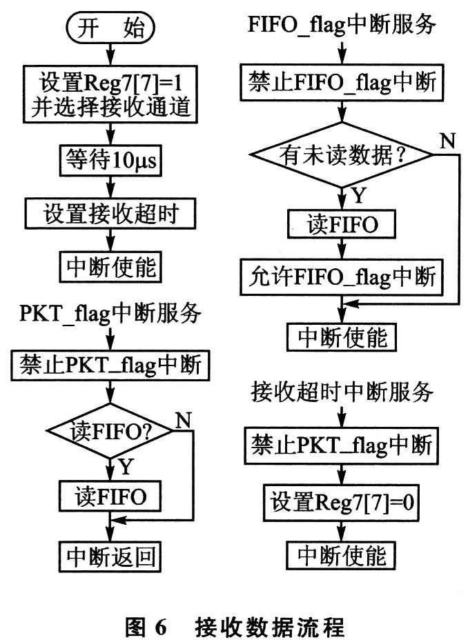
In the design of ultra-low power consumption, MSP430F247 can set a timer interrupt. Usually in LPM3 or LPM4 mode, a timer interrupt is generated when data is to be sent, and EMl98-810 is controlled to be in standby or sleep mode. MSP430F247 works in LPM3 mode and the current is O. Around 8μA, the current is about 0.1μA in LPM4 mode. Under normal circumstances, EMl98810 has a transmitting current of 26 mA, a receiving current of 25 mA, and a standby current of 1.9 mA; in sleep mode it is 3.5 μA. If EMl98810 is set to sleep mode and MSP430F247 is set to LPM3 mode, the system power consumption is only 4.3μA, and it is completely feasible to use dry battery power supply.
MSP430F247 is connected to EMl98810 through SPI interface. The procedures for entering LPM3 mode and exiting LPM3 mode are as follows: 
Set the second bit of Reg48 of EMl98810 to 1 and set SPI_SS to high level to enter sleep mode; if SPI_SS is set to low level again, EMl98810 will automatically wake up and exit sleep mode.
Conclusion After the actual circuit connection test, when the data sending terminal continuously transmits data at a rate of 500kbps, the current of the entire system is 28.2 mA, and the current of the receiving data terminal is 26.1 mA; when the transmitter enters sleep mode, the current is 5.2μA; when the receiver enters standby state LPM3, the current of the whole system is l. 9 mA. According to the calculation of the capacity of 2 dry batteries of 1 300 mAh, 100 bytes of data are sent at intervals of 1 min. Considering the mode switching time of the single-chip microcomputer, at a rate of 500 kbps:
The time required to send data is 5 ms, 1 hour energy consumption:
28.2mA × 5ms × 60 times = 8460 (mA · ms)
1 hour energy consumption in sleep mode:
5.2μA × 3600S × 1000ms = 18720 (mA · ms)
The working time in the sending state is:
(1300mA × 3600S × 1000ms) ï¼ (18720 + 8460) = 172185h
That is, it can work for 20 years when powered by 2 dry batteries. Similarly, it can be calculated that 683 hours (approximately 28 days) can be worked in the receiving state. Therefore, this design can be suitable for long-term low-power wireless data acquisition applications.
Design strategy of ultra-low power wireless data transmission system based on RF2.4GHz
According to the design strategy of ultra-low power wireless data transmission system based on RF2.4GHz At present, wireless communication technology has become a hot spot, and the miniaturization of system design and low power consumption have become an inevitable trend of development. Under the premise of ensuring the reliability of the system, how to achieve low power consumption is a major problem to be solved in the wireless data transmission system. In this paper, a low-power wireless data transmission system is designed by using MSP430 ultra-low power single chip microcomputer and 2.4 GHz ISM band radio frequency chip EMl98810. The system is powered by dry batteries and can be widely used in battery-powered automated data collection systems, wireless remote control, wireless mice, wireless keyboards, wireless electronic tags, remote control toys, and wireless remote transmission automatic meters for water meters, gas, heat, electricity, etc. Meter reading.