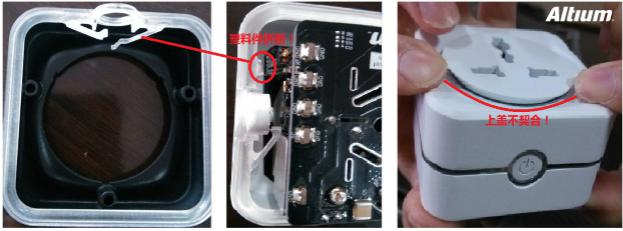
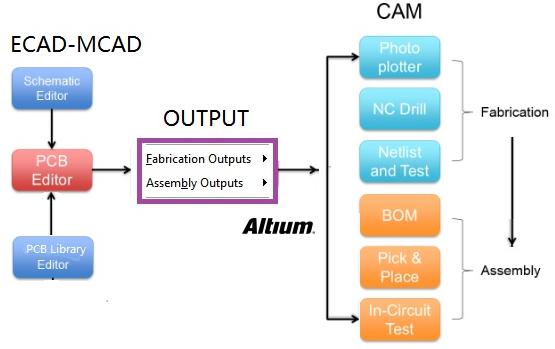
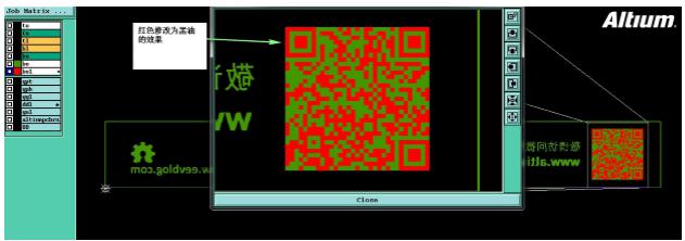
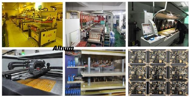
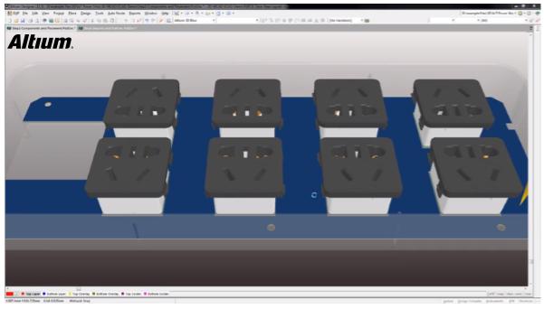
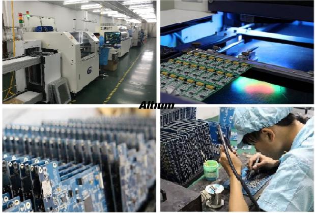
The birth of a perfect electronic product Only good PCB design is not enough. As good as a flower lined with brocade, a good horse with a good saddle; good birds choose wood and habitat, the magi choose the Lord and things. The electronic parts of the PCB that carry your wonderful design inspiration also need to be matched with the precise mechanical parts and the design of the housing. It also requires careful handling and polishing of the PCB board manufacturing and assembly. The organic cooperation between these various teams can successfully deliver a perfect electronic product.       The cooperation between the electronic and mechanical design teams through the 3D component library throughout the PCB design. Also included is the design of the mechanical enclosure matching the design later. The manufacturing and assembly process also requires a bill of materials (BOM) for the design data, as well as compliance with the design requirements and mechanical requirements of the electronics section. The organic cooperation of these teams will greatly increase the product's success rate, shorten product development time, and effectively avoid many hidden problems. PCB Design Electronics and Machinery       In the PCB circuit board design, it is inevitable that there are components to be attached, so it is absolutely necessary to consider the mechanical dimensions of the components and the size and height of the components in order to achieve an accurate PCB layout design. The entire board shape and corresponding mounting holes also need to match the mechanical housing. And need to be manufactured in accordance with PCB, after the assembly is completed, the three-dimensional position of the physical circuit board to ensure the fit of the mechanical shell. Under normal circumstances, electronic design and mechanical design team can not be well unified and interactive data in real time, the following experience you will be familiar with and deeply distressed. For example, you will manually measure the relevant dimensions of the components to implement the component PCB package design:       Then, when you need to use multiple PCBs to be nested together, you need to accurately calculate the size of the groove that each PCB board needs to be removed, and the corresponding position, so as to avoid assembly.       Next, when the circuit boards are all manufactured, assembled, and tested, it is necessary to manually and visually inspect their components and components, and whether there is a spatial conflict between the boards and the boards. As shown in the figure below, are the PCB pins in the horizontal and vertical directions fit? Are large energy storage capacitors and relays placed in space in conflict with other objects? Is the WIFI-controlled smart power outlet's three metal blade size design reasonable? Does the mounting between the board and the board match? Only the matching of these electronic and mechanical parts leads to numerous rounds of PCB circuit board design and mechanical mechanical design corrections. !       Then, the entire electronic circuit of the assembled PCB circuit board is matched with the product casing. There is a transparent belt made of transparent plastic in the middle of the shell of the intelligent power socket, as shown on the left of the figure below. The transparent belt has two photosensitive heads facing the power button. The two photosensitive heads correspond to two LED lights on the erected PCB. The effect of the product is that the LED lamp emits RGB bands of different colors depending on the state, and night lights can be used at night. Unfortunately, due to space conflicts, the plastic photosensors have broken one! ! . Finally, when the entire housing was installed, it was found that there was a gap between the top cover and the whole, which did not fully match the match! !        These problems are not a problem in AlTium Designer. Parents all understand Oh! The STEP model is created automatically when the component library is created to ensure the spatial fit of the components on the PCB. Then there is ECAD-MCAD collaboration to ensure the matching between the electronic core and the mechanical shell of the entire product. PCB design and manufacturing       After the PCB design is completed, it is necessary to output the required files to the downstream PCB manufacturing and assembly. The output is divided into two major parts. One is FabricaTIon Outputs, which is the manufacturing file output. One is Assembly Outputs which is the assembly file output.         The manufacturer of the board knows the drawing data required for the printed circuit board based on the Gerber file or ODB++ file data output by the AlTIum Designer. NC drill drill information, netlist and test data, etc. are also needed. These required documents and data need to be packaged and sent to the board, with the processing requirements. Based on the data obtained and the processing requirements of the plate making process, the board will issue a list of questions and communicate with the engineers. As shown below. Confirm the color of the screen printing QR code on the PCB.      In order to communicate effectively during validation, Alitum's Draftsman document logging tool is used for effective communication and intent transfer. After the two parties have reached a consensus, they can carry out follow-up processes such as PCB production, processing and testing. The following diagram shows the equipment required for the production of the listed PCB manufacturing plants. There are many processes and equipment required for PCB processing. Here, only two or three automatic production line equipments are selected to give you a general impression. Specific details of the production process and complex technical details please refer to the professionals of the processing plants. PCB design and assembly        From PCB design to manufacturing, PCB design to assembly also requires Assembly Outputs, or assembly files, that AlTium Designer packs out to the assembly plant. Contains BOM material list information, Pick and Place placement machine required files, and In Circuit Test (ICT test) files. In fact, inside the Altium Designer software, the PCB layout and wiring stage has been matched to the entire product component model and the product housing and other mechanical parts to ensure that the selected component type and size are correct, to ensure the electronic core and product after the PCB assembly of the product. Machining shell matches. As shown in the figure below, this power strip contains 8 power outlet modules. The electronic parts inside each module (resistance and capacitance relay transformers and other electronic components and PCB circuit boards) are perfectly matched with the corresponding mechanical enclosures .        Therefore, in the PCB assembly production, as long as the processed BOM and the BOM list of the electronic components and other components purchased according to the design requirements are clear and quality is guaranteed, component placement and welding are performed according to the Pick and Place document, and As other components are assembled, the process becomes standard and accurate. After all components are assembled, ICT circuit testing and functional testing are performed. See the figure below for related equipment of some assembly lines. PCB assembly is divided into SMT chip components, soldering; connector part placement, welding; product testing; surface treatment and adding protective coating; product packaging (some will be assembled together with the product mechanical enclosure). During the PCB assembly process, Altium Designer design software needs to provide an accurate BOM list, pick and place files, stencil files, and more for automated placement. In addition, it is also necessary to cooperate with the assembly manufacturers to provide product test files, and configure the test rack to test the product yield rate.        If the data between PCB electronic design, mechanical design, manufacturing, and assembly teams cannot be shared in real time and work in a coordinated manner, after the assembly production is completed, once the electronic part of the product is found to not match well with the mechanical housing, Either re-edit the electronic PCB part or re-modify the mechanical housing part design. No matter what part of the revision, it is necessary to change the design data again, then process the production, and then finally match, so that the problems and changes once and for all are a torment to all teams. Therefore, for a perfect electronic product, to avoid such time-consuming and laborious multiple iterations, it is necessary to integrate the various teams organically at the design stage, share the required data, and achieve organic cooperation among all team members. To avoid data errors and possible problems. Shenzhen Zpal Technology Co.,Ltd , https://www.zpal-vape.com