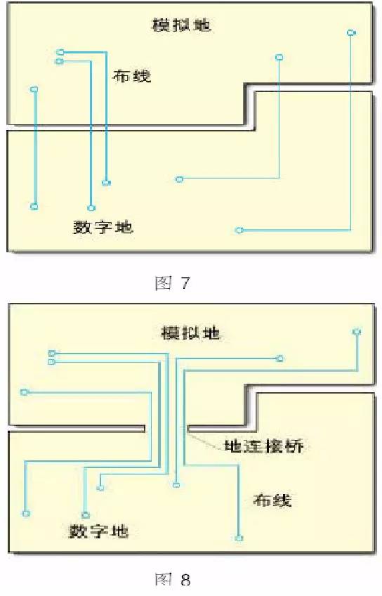
1. The structure of the structural layer of the ply is a very important factor in determining the EMC performance of the system. A good lamellar structure has a good effect on suppressing radiation in the PCB. Multilayer boards are often used in high-speed circuit systems that are common today, rather than single and double panels. Pay attention to the following aspects when designing multiple panels. 1. A signal layer should be adjacent to a copper layer; How to reduce the mutual interference between digital signals and analog signals? There are two basic principles: the first principle is to reduce the area of ​​the current loop as much as possible; the second principle is that the system uses only one reference plane. Conversely, if the system has two reference planes, it is possible to form a dipole antenna (note: the radiation size of the small dipole antenna is proportional to the length of the line, the magnitude of the current flowing, and the frequency); and if the signal cannot pass as much as possible With a small loop return, it is possible to form a large loop antenna (note: the size of the radiation of the small loop antenna is proportional to the loop area, the current flowing through the loop, and the square of the frequency). Avoid both situations. It has been suggested to separate the digital ground and the analog ground on the mixed-signal circuit board to achieve isolation between the digital ground and the analog ground. Although this method is feasible, there are many potential problems, and the problem is particularly acute in complex large systems. The most critical issue is that it is not possible to route across the split gap. Once the split gap wiring is crossed, electromagnetic radiation and signal crosstalk increase dramatically. Problem: The most common problem in PCB design is the EMI problem caused by the signal line crossing the split ground or the power supply. Solution: Understanding the path and mode of current flow back to ground is key to optimizing mixed-signal board design. Many design engineers only consider where the signal current flows, ignoring the specific path of the current. If the ground layer must be split and must be routed through the gap between the splits, a single point connection can be made between the divided grounds to form a bridge between the two grounds, and then route through the bridge. In this way, a direct current return path can be provided below each signal line, resulting in a small loop area. Signals can also be used to span the split gap using optically isolated devices or transformers. For the former, the optical signal is crossed across the gap; in the case of a transformer, it is also possible to use a differential signal across the split gap: the signal flows from one line and returns from the other. Next, it is not required as a return path. In practice, it is generally preferred to use a uniform, partitioned PCB into analog and digital parts. The analog signal is routed in the analog area of ​​all layers of the board, and the digital signal is routed in the digital circuit area. In this case, the digital signal return current does not flow into the ground of the analog signal, only the digital signal is routed on the board. The interference of the digital signal to the analog signal occurs when the analog portion is overlaid or the analog signal is routed over the digital portion of the board. This problem does not occur because there is no division. The real reason is that the digital signal wiring is not appropriate. When connecting the analog ground and digital ground pins of an A/D converter, most A/D converter manufacturers recommend connecting the AGND and DGND pins to the same low-impedance ground through the shortest leads. If the system has only one A/D converter, the above problem can be easily solved by dividing the ground. When the analog ground and the digital ground are connected together under the A/D converter, the method must be ensured. The width between the bridges is as wide as the IC, and no signal lines can cross the split gap. If there are more A/D converters in the system, for example, how do 10 A/D converters connect? If the analog ground and the digital ground are connected together under each A/D converter, a multi-point connection is produced, and the isolation between the analog ground and the digital ground is meaningless. If you do not connect in this way, it violates the requirements of the manufacturer. The best way is to use uniforms at the beginning. Dividing the unified ground into an analog part and a digital part, such layout and wiring meets the requirements of the IC device manufacturer for the low-impedance connection of the analog ground and the digital ground pin, and does not form a loop antenna or a dipole antenna. EMC problem. Mixed-signal PCB design is a complex process, and the design process should pay attention to the following points: For Figure 7 and Figure 8, what are the specific characteristics of the distribution of these two types of land? I found some problems in the ring on the Internet. The suggestion is to make the ground of the switching power supply. What they recommend is to connect the ground of the BUCK power supply to the ground of the digital circuit. As for the specific role and meaning of this treatment, my understanding is rather vague. I don't know how you look at the processing of the BUCK switching power supply. Suppose we split Ground A and Ground B as shown in Figure 1, and use the model of the transmission line to equate Slot. When the signal line enters Ground B through Ground A, since there is no continuous return path between A and B, the signal transmission line induces a negative flowing charge on Ground A (the flow of negative charge forms a signal return on Ground A). ), these negative charges cannot reach Ground B. Then the corresponding positive and negative charges are polarized on Ground B. The negative charge induced on Ground B and the signal line above it constitute the reflow of the signal, while the positive charge induced will be along with the negative charge of a part of Ground A along the Slot's transmission line model at the intersection of the signal line and the Slot. Transfer on both sides. The current shown by the current source shown in Figure 2 is simultaneously transmitted in both directions through the Slot transmission line. Then the remaining negative charge of Ground A will be reflected back to the drive end of the signal on Ground A. Two of the circuits are the parasitic capacitances of the transmission line formed on the upper edges of the two copper layers. The transmission line on the Slot width is replaced by an inductance model. The validity of this model has been proven [2]. This allows some of the characteristics of signal transmission to be known. Where T is the transmission coefficient of the signal transmission line and R is the reflection coefficient of the signal. X: is the mode conversion coefficient. It is the ratio of the voltage value of the transmission line model flowing to the Slot to the voltage value on the original signal transmission line. When the frequency is low or Lx and Cx are negligible, the above formula can be simplified as: At the same time, the attenuation of energy is also very serious when the signal line passes through the Slot. Another simulation diagram is shown in Figure 3. The specific parameters are as follows: Microstrip Line Trace Width = 0.3 mm; Trace Length = 8.2mm; Gap Width = 0.6 mm; Gap Length = 6.0 mm; PCB Thickness = 0.13 mm, FR-4; Frequency: 0 - 5GHz The plot is generated at 5GHz. The software used is Ansoft HFSS 8.0. It can be seen that because no conductor provides a return path, the current has to skip the gap and a lot of energy is lost in the process. Some of the energy lost is radiated into the air, and some energy travels along the gap. If there is another Trace across the gap, there will be a serious Crosstalk. Therefore, in the layer design, the situation that the signal line crosses the Slot should be avoided. Otherwise it will produce very severe EMI. If some signal lines must pass through the span, it is effective to place a bypass capacitor at the cross-section. The PCB board of the signal source has 6 layers. It is divided into 4 signal layers and two copper-clad layers (second and fifth layers). The working power supply has both digital and analog power and is 5V. Therefore, a simulated power supply area is designed on the surface layer, and a simulated ground area is divided in the second layer (ground copper), and a single point connection is adopted. A filter is formed at the junction using magnetic beads and capacitors in series, as shown in Figure 4. The device in the figure is a PLL clock generator and is a digital-to-analog device. In order to provide the grounding pin and the ground pin with minimum impedance to ground, a DGND copper is directly applied under the device because this copper can be regarded as a ground wire with less inductance. At the same time, multiple bypass capacitors are placed between DGND and DVDD. The magnetic beads FB1, FB2 and two capacitors are used between the digital and analog power supplies (ground) to form a series LC filter. This provides a more stable and reliable power supply for the digital-to-analog device. 3.3, 20H rules often use the "20H" rule in the design of the power layer. The meaning is that the ground copper layer is epitaxial 20H relative to the power supply copper. Where H is the dielectric thickness between the power supply and the ground copper. However, in actual high-speed circuits, it is necessary to decide whether or not the 20H rule should be used according to different situations. The 20H rule can significantly reduce external radiation when there are only two copper-clad (Power and Ground) structures in the PCB layer. However, the effect of the 20H rule is not obvious for a plurality of copper-clad laminate structures; however, external radiation can be significantly reduced by using vias. Figures 5 and 6 below are simulations for two copper-clad and multiple copper-clad laminate structures. It can be seen from the above two simulation diagrams that the 20H rule is applicable to two copper-clad Power-Ground structures; and the via holes are excellent for suppressing radiation in a plurality of copper-clad structures. Of course, the use of vias also requires detailed research. Excessive vias increase the impedance of the copper layer and destroy the continuity of the copper layer.
Not only fashionable, but also protective. Our protective sleeves provide impact protection, shock absorption and a slim design. The Phone Case can give you peace of mind and provide better protection. If you keep your phone clean and scratch-free, you can also increase the resale value of your phone.
Design: The fit design makes your phone slimmer.
Protection: These Mobile Phone Case have been tested to withstand those accidental drops. The inner layer is made of Soft TPU rubber material, and the reinforced corners can absorb impact. High lips recess your screen and camera to provide additional protection. The outer hard shell is impact resistant.
Function: When all ports can be accessed, your phone can be used normally. The Cell Phone Case has molds for volume buttons and power buttons, so it is protected and you can still feel/use them.
If you want to know more about Mobile Phone Case products, please click the product details to view the parameters, models, pictures, prices and other information about Mobile Phone Case.
Whether you are a group or an individual, we will try our best to provide you with accurate and comprehensive information about the Mobile Phone Case!
Matte Phone Case, Marble Phone Case, Protective Case, Iphone Case, Transparent Phone Case, Protective Cover Shenzhen Jianjiantong Technology Co., Ltd. , https://www.jjthydrogelprotector.com
2. The signal layer should be tightly coupled to the adjacent copper layer (ie, the thickness of the medium between the signal layer and the adjacent copper layer is small);
3. Power supply copper and ground copper should be tightly coupled;
4. The high-speed signal in the system should be in the inner layer and between the two copper layers, so that two copper coatings can shield these high-speed signals and limit the radiation of these signals to two copper-clad areas;
5. Multiple layers of copper can effectively reduce the impedance of the PCB and reduce common mode EMI.
(1) PCB partition is an independent analog part and a digital part
(2) Appropriate component layout
(3) A/D converter is placed across partitions
(4) Do not divide the ground: lay it uniformly under the analog and digital parts of the board
(5) In all layers of the board, digital signals can only be routed in the digital portion of the board; analog signals can only be routed in the analog portion of the board.
(6) Implement analog and digital power splitting
(7) Wiring cannot cross the gap between the split power planes
(8) The signal line that must cross the gap between the divided power supplies should be located on the wiring layer next to the large area.
(9) Analyze the path and method of the actual return current
(10) Adopt the correct wiring rules
Circuit measures in PCB design When designing electronic circuits, we consider the actual performance of the product, and do not consider too much the electromagnetic compatibility characteristics of the product and the suppression of electromagnetic disturbance and the electromagnetic anti-interference characteristics. In order to achieve electromagnetic compatibility for the PCB layout, the necessary circuit measures must be taken, that is, the necessary additional circuits should be added on the basis of the circuit schematic to improve the electromagnetic compatibility of the products. The actual PCB design can be used. The following circuit measures:
(1) It is possible to reduce the rate of the lower edge transition of the control signal line by connecting a resistor in series on the PCB trace.
(2) Try to provide some form of damping for relays, etc. (high frequency capacitors, reverse diodes, etc.)
(3) Filter the signal entering the printed board, and filter the signal from the high noise area to the low noise area, and reduce the signal reflection by using the serial termination resistor.
(4) The useless end of the MCU should be connected to the power supply or ground through the corresponding matching resistor or defined as the output terminal. The power supply and ground terminals on the integrated circuit must be connected. Do not hang.
(5) The input terminal of the unused circuit is not left floating, but is grounded through the corresponding matching resistor or the grounded idle input of the op amp. The negative input is connected to the output.
(6) Set a high frequency decoupling capacitor for each integrated circuit. Add a small high frequency bypass capacitor to each electrolytic capacitor.
(7) When using a large-capacity tantalum capacitor or a polyester capacitor instead of an electrolytic capacitor as a charge and discharge storage capacitor on the circuit board, when the tubular capacitor is used, the outer casing should be grounded. 
Question: "There is also a feasible way to use differential signals: the signal flows from one line and returns from the other. In this case, it does not need to be the return path." A: The differential signal is actually dominated by the ground loop. The return path, only a small portion returns from the other line number. Assuming an extreme case, if the main return path of the differential signal is another signal line, then we can cut off the ground plane (power plane) below the differential line. And I feel that if this is done, the return path and effect will definitely be problematic. Partial reflow cancellation of the ground plane does not mean that the differential circuit does not use the reference plane as the signal return path. In fact, in signal reflow analysis, the mechanism of differential traces and ordinary single-ended traces is the same, that is, high-frequency signals are always reflowed along the loop with the smallest inductance. The biggest difference is that the differential lines have coupling to ground. In addition, there is a mutual coupling, which is strong, and that becomes the main return path. In the PCB circuit design, the coupling between the differential traces is generally small, often only 10 to 20% of the coupling degree, and more is the coupling to the ground, so the main return path of the differential traces still exists in the ground plane. . When the local plane is discontinuous, there is no reference plane, and the coupling between the differential traces will provide the main return path, although the discontinuity of the reference plane does not affect the common single-ended trace. It is serious, but it will reduce the quality of differential signals and increase EMI. Try to avoid it. Some designers believe that the reference plane below the differential trace can be removed to suppress some of the common-mode signals in the differential transmission, but in theory this approach is not advisable. How is the impedance controlled? Not providing a ground impedance loop for the common mode signal will inevitably cause EMI radiation, which is more harmful than good. Question: Is it more important to keep the spacing of the differential traces longer than the matching line length?
A: In actual PCB layout, it is often not possible to meet the requirements of differential design. Due to factors such as pin distribution, vias, and routing space, the wire length matching must be achieved by proper winding, but the result is necessarily that the partial regions of the differential pair cannot be parallel. The most important rule in the design of PCB differential traces is the match line length. Other rules can be flexibly processed according to design requirements and practical applications. Question: Is the differential trace necessarily close enough? A: Let the differential traces be close to each other in order to enhance their coupling, which can improve the immunity to noise and make full use of the opposite polarity of the magnetic field to offset the electromagnetic interference to the outside world. Although this practice is very beneficial in most cases, it is not absolute. If we can guarantee that they are fully shielded from external interference, then we do not need to let the strong coupling through each other to achieve anti-interference. And the purpose of suppressing EMI. How can we ensure that the differential traces have good isolation and shielding? Increasing the distance from other signal traces is one of the most basic ways. The electromagnetic field energy decreases with the square of the distance. When the line spacing is more than 4 times the line width, the interference between them is extremely weak. Can be ignored. In addition, the ground plane isolation can also be used for good shielding. This structure is often used in high-frequency (10G or more) IC package PCB design. It is called CPW structure and can guarantee strict differential impedance. Control (2Z0). Differential traces can also be used in different signal layers, but this method is generally not recommended because differences in impedance, vias generated by different layers can disrupt the effects of differential mode transmission and introduce common mode noise. In addition, if the adjacent two layers are not tightly coupled, the ability of the differential traces to resist noise is reduced, but crosstalk is not an issue if the proper spacing from the surrounding traces is maintained. At normal frequencies (below GHz), EMI is not a serious problem. Experiments show that the differential excitation of 500Mils, the radiant energy attenuation of 3 meters away has reached 60dB, enough to meet the FCC electromagnetic radiation standard, so The designer does not have to worry too much about the electromagnetic incompatibility caused by insufficient coupling of the differential lines. Most of the ply structure arrangements shown in the above four tables do not fully comply with the above five points. This requires the selection of the appropriate layer structure according to the actual system requirements. The following is a description of the commonly used 6-layer board structure.
A: The 2nd and 5th layers are power and ground copper. Due to the high impedance of the power supply copper, it is very unfavorable for controlling common mode EMI radiation. However, from the point of view of signal impedance control, this method is very correct. Because of this layer design, Layer1 and Layer3, Layer4 and Layer6 of the signal routing layer constitute two pairs of reasonable wiring combinations.
B: The power supply and the ground are placed on the 3rd and 4th layers respectively. This design solves the problem of the copper impedance of the power supply. Due to the poor electromagnetic shielding performance of the first layer and the sixth layer, the differential mode EMI is increased. This design can solve the differential mode EMI problem if the number of signal lines on the two outer layers is the least and the trace length is short (shorter than the 1/20 of the highest harmonic wavelength of the signal). The suppression of differential mode EMI is particularly good when copper is filled with no components and no trace areas on the outer layer and the copper area is grounded (interval every 1/20 wavelength).
C: From the perspective of signal quality, it is clear that the layer arrangement in the C case is the most reasonable. Because such a structure is ideal for the path of high frequency reflow of the signal. But this arrangement has a more prominent shortcoming: the signal has fewer layers. So such a system is suitable for high performance requirements.
D: This enables the environment required for signal integrity design. The signal layer is adjacent to the ground layer, and the power layer and the ground layer are paired. Obviously, the downside is that the structure of the layer is unbalanced (unbalanced copper coating may cause warpage of the PCB). The solution to the problem is to apply copper to all the blank areas of the third layer. If the copper density of the third layer is close to the power layer or the ground layer after copper plating, the board can be regarded as a structurally balanced circuit board. . The copper area must be connected to power or ground. Most of the 8-layer boards currently in use are designed to improve the signal quality of the 6-layer board. It is known from Table 3 that the 8-layer board has no wiring layer for adding signals compared with the 6-layer board, but two additional copper-clad layers are added, so that the EMC performance of the system can be optimized.
2. Parameters of the plate layer The parameters of the plate layer include the line width of the signal trace, the line thickness, the medium between the signal layer and the copper layer, and the thickness of the medium. The determination of the ply parameters is mainly based on factors such as the impedance control of the signal and the manufacturing process limitations of the PCB. Of course, frequencies above GHz also need to focus on the skin effect of the transmission line and the loss of the medium. For the commonly used medium FR-4, the medium has a significant attenuation of the signal at ≥ 1 GHz. The impedance of the signal line is mainly limited by a number of parameter variables, which can be simply described by the following formula.
Of which: Z. Is the impedance of the signal line; w: is the line width of the trace; h: the line height of the trace; H: the thickness of the medium; ε: the dielectric constant of the medium. Among these parameter variables, H has the greatest influence. The impedance of the transmission line can usually be calculated using the POLAR CIT25 software. There are also some differences in the parameters required for the calculation of different transmission line types (microstrip lines and strip lines, etc.).
3. Design of the power (ground) layer Before studying the design of the power (ground) layer, it is necessary to know the reflow problem of the high frequency signal. The principle of reflow of high frequency signals is to return the drive end of the signal along the path with the least impedance. At the same time, the reflow of the signal is different when the waveform of the signal is switched. The signal return of the transmission line on the PCB always forms a current return path along the copper that is closest to the transmission line, but differs when approaching the drive end of the signal. If the signal output is logic high, the return of the signal must enter the power supply pin of the driver. Conversely, if the output is low, the return of the signal must be back to the ground pin of the driver. High capacitance and low inductance are required between the transmission line and the return path of the signal. A high capacitance is better for including the electric field; a lower inductance is for reducing the magnetic flux that passes through. In the study of the problem of reflow of high-frequency signals, the design of the power supply will be studied in detail below.
3.1. Power (ground) layer division Now that the system's working power supply is mostly multiple power supplies, it is necessary to study the power (ground) layer segmentation (Slot) problem in actual operation. Knowing from the signal reflow problem studied above, Slot makes the return path of the signal difficult to control. If the signal cannot be returned through the loop as small as possible, it is possible to form a large loop antenna (the size of the radiation of the small loop antenna is proportional to the loop area, the current flowing through the loop, and the square of the frequency). Of course, from another perspective, Slot is good for noise isolation and can prevent mutual interference between different partitions. The division of the power (ground) layer will be studied in detail below.
3.2, digital-mode power supply design The main purpose of digital-analog power supply design is to reduce the interference of digital signals (digital power) to analog signals (analog power). At the same time, we need to pay attention to two aspects. First: reduce the area of ​​the current loop as much as possible; second: the system uses only one reference plane. If the system has two reference planes, it is possible to form a dipole antenna (the radiation size of the small dipole antenna is proportional to the length of the line, the current flowing through it, and the frequency). Therefore, the connection between the digital-mode power supply and the ground-clad copper is a single-point connection. This allows for the formation of a reference ground copper and also prevents the formation of a small loop loop between the digital analog grounds. Because such a return loop is a factor in generating ground bounce noise. Because if a multi-point connection is used, noise can form more loops through multiple connection points. The single point connection point should be below the digital-analog mixing device. At the same time, it is necessary to pay attention to the connection mode of the digital mode. Considering the isolation of noise, the digital-analog hybrid connection is connected by magnetic beads, and the magnetic beads can be connected to each other through DC. So this prevents some high frequency noise from entering the analog area. Because digital devices have noise margins, analog devices are very sensitive to noise. Let's take a narrative with the design of an example.