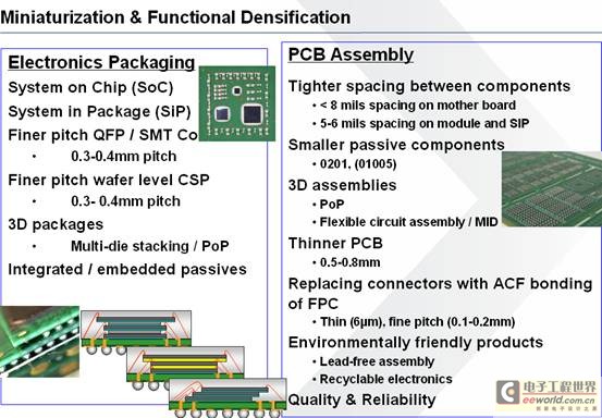
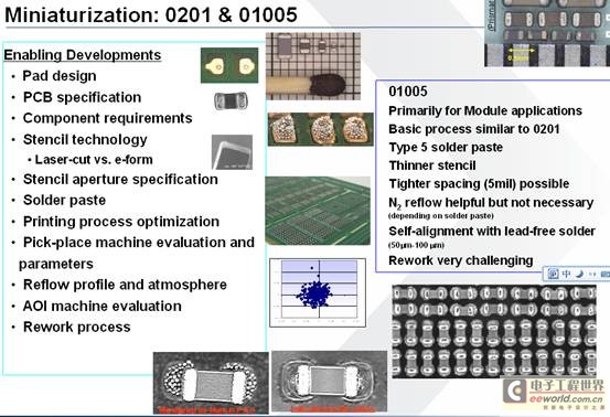
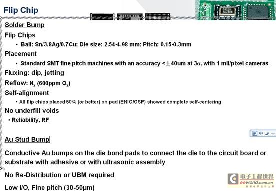
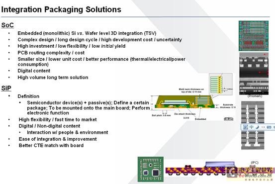
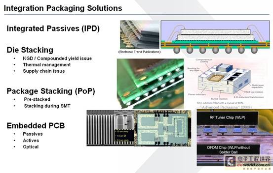
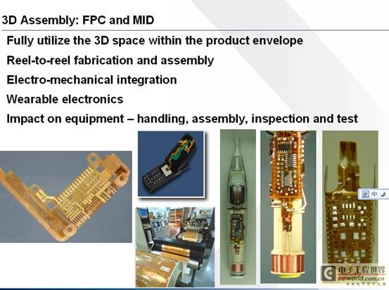
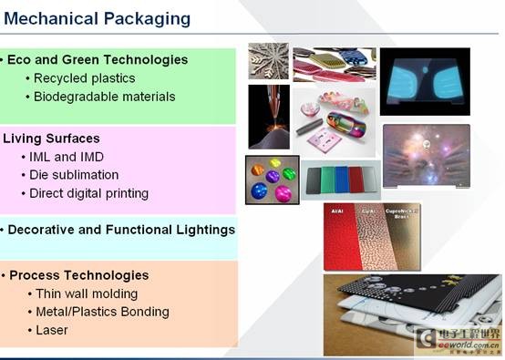
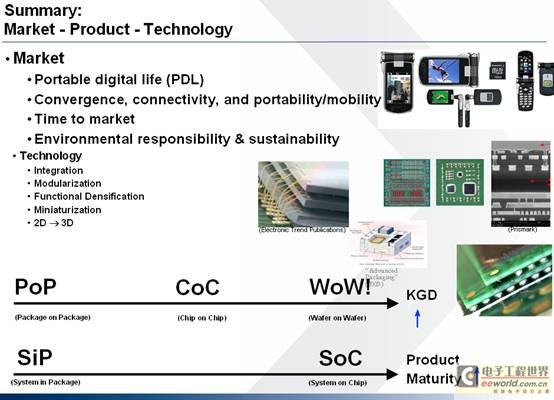
In the 3rd China International Medical Electronics Technology Conference (CMET2010) process workshop held recently, Dr. Shangguan Dongyu, Senior Vice President of Technology Department of Flextronics Headquarters, gave a wonderful speech titled "Miniature Packaging and Assembly Technology in Medical Electronics" Presentations and interactive discussions with medical audiences on medical electronics, especially in portable, home-based medical electronics manufacturing processes. Product miniaturization technology has been developed and applied for many years in other products, such as consumer electronics such as mobile phones, and related experiments have been around for several years. In the CMET2010 process workshop, Dr. Shangguan Dongyu combined with Flextronics' many years of experience to introduce the application of miniaturization technology in medical devices. Flextronics' assembly capability There are many microelectronic packaging technologies that can be applied to medical devices. For example, integration, including integrated silicon for semiconductor silicon, system in Package, and three-dimensional packaging. As well as assembly, there are less than 8 mm, or 0201, 01005 components assembly, three-dimensional assembly, flexible circuit board assembly, etc., at the board level, these methods can also achieve miniaturization of the product. Miniaturized packaging and assembly technology that can be used in medical electronics Specifically, taking the assembly of 0201 and 01005 components as an example, this technology has been applied in consumer electronics for five years, but it has not been widely used in medical electronics because it involves micro-devices in terms of process. Higher requirements: such as device requirements, PCB board requirements, device flatness, printing process requirements, etc. And need to consider the design and manufacturing after the test, as well as the final repair and so on. Therefore, some work needs to be done before this technology can be applied to medical equipment. 01005 is mainly the application of the module. The basic process is very similar to 0201, but it should be further refined in the process. For example, in the selection of solder paste, it may be necessary to use nitrogen during soldering, and it may be very difficult to repair. . There are also many types of Flip Chips, such as the Solder Bump can be up to 150 microns. There are many things that need to be done to implement Flip Chips in the product, what are the requirements of the equipment, what are the requirements of the process, and so on. Fluxing is difficult to use with Flip Chip because of the very fine pitch, and Reflow requires nitrogen. Nitrogen does not have to get 50 PPIs. More use of Au Stud Bump, the easiest way to further miniaturization is Au Stud Bump. There are also a number of other integrated approaches, such as SOC and SIP. When to use SOC, when to use SIP has some controversy. SOC is generally a mature product, mature design, and mature market. Because of the high cost of SOC, only batch applications have an advantage. SIP is generally used in the application of new technology products because it is relatively low cost and faster to implement, and is more suitable for new products and new technologies. In addition, some devices can be directly integrated into the silicon, and Die Stacking is familiar to everyone. We usually have to consider the use of silicon wafers. If the field is relatively low, stacking several ones together will eventually be a layered consideration. Also, Package Stacking is familiar to everyone. For example, Embedded Components in PCB, further miniaturization, increases its functionality and density. From a functional point of view, especially for high quality applications, it is desirable that the distance between the PCB and the silicon wafer be as good as possible. There are some considerations from Embedded Components in PCB and Flip Chip. There is still a lot of discussion and debate on this issue. Because of its impact on cost, we will gain some advantages in terms of miniaturization and product functionality, but at the same time have some impact on manufacturing costs. There is still no clear thing about how to make this decision. Just now we have been talking about devices and microelectronics, from the board-level packaging, assembly, what are the high-density assembly and fine pitch devices. The fine pitch between the devices, there are important factors to consider here. For example, PCB board design, PrinTIng, the spacing is getting thinner and more dense, how to pull this line out. There is also a Pick-place, Reflow in air aspect. Now that you have a very dangerous device, there is a higher one, a bigger one, which one you put first, and these specific things must be considered for optimization. Three ways to assemble three-dimensional, one is Package, we use in-line, this process was made in 2002 at Flextronics Lab, and applied to the large-scale production application of Xixiang factory in 2003. Because at that time the process was called Package Stacking. What did we do in 2002? In fact, do management and do in-line, and do both at the same time. This process has not been used in larger applications in industry until 2005 or 2006. What are the benefits of this? Mainly from the Aspects of Package Stacking, there is more flexibility, it can be two management, and now it is used in almost all mobile phones. I think it can be applied to this foundation in the miniaturization of medical devices. What other ways to do three-dimensional assembly? There is a lot of space inside the product that has not yet been utilized. We are going to do miniaturization now. To increase the functional density, how can we use more space for the product? Flexible boards offer us the opportunity. Picasso once said that all you can imagine is real. In the above-mentioned technological advancement of miniaturized packaging and assembling flexible circuit boards, this sentence can also be understood as: all the products you can imagine are: Can be produced. It is not enough to produce it alone, and medical equipment needs higher reliability. Miniaturization and high-density packaging pose challenges for reliability. Such as electrochemical reliability, thermal reliability, solder joint reliability, dynamic load reliability and so on. In addition, there are problems with packaging materials and appearance. Now there are many environmental protection regulations. Therefore, it is necessary to adopt ecological and green technologies, recycled plastics, biodegradable materials, and take into account the consumer experience and adopt more beautiful packaging. The last issue to be aware of is DFX, which is a manufacturable design. There are a lot of designs in the room, and many of them are made. How to integrate design and manufacturing? How to cooperate? The answer is through DFX. The design of the product is now more than just a question of the design team, but also the involvement of the manufacturing team. But this is not the main challenge. Where is the challenge today? Everyone knows that today is a global environment. The design team may be a design and development center in one place of a certain company, but it may be a manufacturing factory in another place of another company. The two companies may use How do different systems implement design and manufacturing cooperation in such an environment? How to optimize the design? This is a subject that the industry must face. Finally, the technology is to be market-oriented. From the trend of the market, home medical electronic products are developing towards consumer electronics, and may require more wireless connections and links to household appliances. The product replacement is fast, and at the same time, it must meet some management requirements. And market requirements. From a technical point of view, integration, modularization, high density, miniaturization, and three-dimensionalization are required. Use these technical means to meet the product requirements of the market. In addition, we need cooperation across the entire supply chain because we don't have time to move from one company to another. Activities such as CMET have greatly promoted the cooperation of the entire industry chain, promoting the entire industry, the cooperation of the supply chain to promote the upgrading of products, and promote cooperation in design and manufacturing. I hope that through this conference today, through the research and discussion of everyone, we can promote the cooperation of the entire supply chain and promote the cooperation between design and manufacturing.