Implement Master-Slave TIming-Card Redundancy Using Maxim TIming ICs Anker Battery Pack,Blackweb Battery Pack,12V Rechargeable Battery Pack,12V Rechargeable Battery Pack Zhejiang Xinghai Energy Technology Co.,Ltd , https://www.headwayli-battery.com Abstract: Telecom equipment with SONET / SDH or Synchronous Ethernet ports must have very high reliability and fault tolerance. One requirement for these systems is dual, redundant TIming cards in a master-slave arrangement. TIming ICs from Maxim Integrated Products not only handle important clock synchronization responsibilities, they also enable the timing card redundancy required for compliance with Stratum 3, G.813 and other telecom standards. This application note explains how to use Maxim timing ICs to implement dual, redundant timing functions in telecom equipment.
IntroductionThis application note describes how to use Maxim timing ICs to implement dual, redundant timing functions in telecom equipment. Designing a system with redundant timing functions for fault tolerance is not merely a good design practice. For systems with clock quality of Stratum 4E or better it is a definite requirement. See Telcordia document GR-1244-CORE for details.
In this document, the term "timing card" refers to a printed circuit board (PCB) that contains one complete, independent, system timing function such as a Maxim DS3100, DS3101, or DS3102 timing IC and its local TCXO or OCXO. Most timing cards are designed so that two identical units can operate in a master-slave arrangement in a multicard, backplane-connected system. At the levels of integration common today, these cards typically do much more than just system timing. Many cards have on board several other functions that also must be implemented with 1: 1 equipment protection, such as system management processors, packet switches and TDM switches. Despite the multifunction nature of these cards, the traditional term "timing card" is used in this document.
Hardware Configuration Connections Between Redundant Timing CardsThe wiring of the timing cards and the system backplane includes a dedicated clock signal from timing card A to timing card B, and a similar clock signal from timing card B to timing card A. See Figure 1.
The frequency of the clock signals cross-wired between the timing cards depends on system requirements. In some systems, all line cards are required to have a common 8kHz frame alignment and / or 2kHz multiframe alignment. In these systems, the frequency of the cross -wired clock signals should be the lowest frequency at which phase alignment is required: 2kHz if multiframe alignment is necessary, 8kHz otherwise. In SDH / SONET systems that do not require frame and multiframe alignment, the frequency of the cross-wired clock signals is typically 6.48MHz or 19.44MHz. In systems with only Synchronous Ethernet ports and no SDH / SONET, a 25MHz frequency is often used.
Connections from Timing Cards to Line CardsIn addition to the cross-wired clock signals between redundant timing cards, one or more system clock signals from each of the timing cards are routed across the backplane to all line cards. Each line card has a line-card timing IC (such as the DS3104, DS3105, or DS3106) that can monitor both system clock signals and automatically switch from the master clock signal to the slave clock signal, if the master clock signal fails. See Figure 1.
Two methods are in widespread use for routing clock signals from timing cards to line cards. The first method uses point-to-point wiring from each timing card to each line-card slot. This method requires more traces on the system backplane, but is the most fault tolerant. The second method is point-to-multipoint wiring from each timing card to the line-card slots. A multipoint version of low-voltage differential signaling called M-LVDS is often used for this. Systems built to comply with the ATCA or micro-TCA standards use M-LVDS to implement this second method, which requires fewer traces on the backplane. 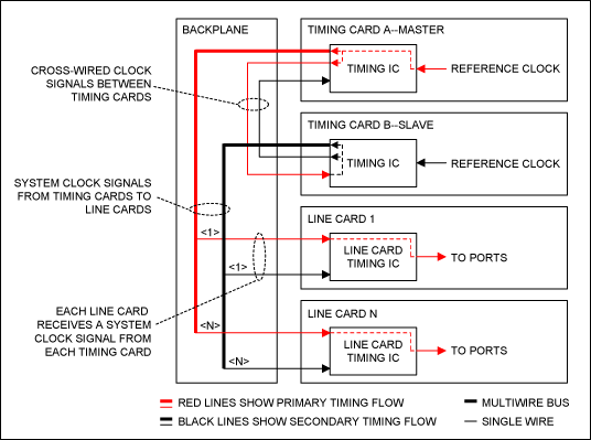
Figure 1. Timing flow before master-slave switching
Initial Device ConfigurationAt system power-up one of the timing cards is arbitrarily chosen to be the master while the other is designated the slave.
The master timing card IC is configured to be the system timing function. It is configured to have a specific priority list of input clocks to select from, an appropriate bandwidth for the application, phase-build-out-on-change-of-reference enabled (PBOEN = 1) to provide hitless reference switching, and any other settings required to comply with the relevant telecom synchronization requirements.
The slave timing card IC is configured only to track the master. The only input clock pin enabled on the slave is the input connected to the master. The bandwidth of the slave is set at least 10x greater than the master's bandwidth so that the slave can Quick follow any phase movement in the master's clock signal. In addition, phase-build-out-on-change-of-reference is disabled (PBOEN = 0) in the slave to ensure that the slave tracks the master with zero phase difference. These settings ensure that the clock signals from the master and slave timing cards are frequency locked and in phase at the line cards. This allows the line-card timing ICs to switch from the master clock signal to the slave clock signal quickly without causing phase changes on the line-card ports.
Master-Slave Switching ProcedureThere are two causes of master-slave switching. The first cause is a failure of the master timing card that causes its output clock (s) to be off frequency by an unacceptable amount or to not toggle at all. The second cause is a management-initiated command to switch the roles of the master and slave timing cards.
When a master timing card fails, the slave timing card IC detects the failure and automatically changes state from locked to holdover. This change instantly isolates its output clocks from the master clock signal that it had been tracking. If the master failure causes its output clock to stop toggling, all the line-card timing ICs detect the failure and automatically switch to the system clock signal from the slave timing card. If, instead, the master failure causes its clock to be off frequency, the slave timing IC can detect this . The line-card timing ICs, however, may not have frequency measurement capability. In this situation, system software can react to an interrupt from the slave timing IC and manually force all line-card timing ICs to switch to the system clock signal from the slave timing card.
If there is a management-initiated command to switch the roles of the master and slave timing cards, the master's clock is still valid and the slave timing card has no reason to automatically go to holdover. Therefore, system software must put the slave timing card IC into holdover manually by setting MCR1.T0STATE = 2.
In all of the above cases, the end result is that the entire system is timed from the slave timing card IC in its holdover state. Because of the stability of the slave's local oscillator, the system can easily operate in this state for the short period of time required to reconfigure the timing ICs as follows: If not already done, force the slave timing IC into holdover (MCR1.T0STATE = 2). If not already done, force all line-card timing ICs to lock to the slave clock instead of the master (use field MCR4.T0FORCE or the SRCSW pin). Disable all clock outputs on the master timing IC and force it into holdover (OCR1 = 0, OCR2 = 0, OCR3 = 0, OCR4 = 0, MCR1.T0STATE = 2). Configure the slave timing IC with exactly the same configuration that the master had before, including input clock priorities, bandwidth, and PBOEN = 1 for hitless switching. Configure the slave timing IC for automatic state transitions (MCR1.T0STATE = 0) rather than forced holdover. The slave is now officially the new master. See Figure 2 . If the line-card timing ICs normally do automatic switching between master and slave system clocks, enable automatic switching by setting T0FORCE = 0 in each device. At this point, if the master-slave switch was caused by a management command, configure the former master to be the new slave, as described in Initial Device Configuration above. If the master-slave switch was caused by failure of the master, leave the former master in holdover with its clock outputs disabled until it can be replaced. 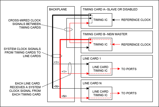
Figure 2. Timing flow after master-slave switching.
With Maxim timing ICs on the timing cards and line cards, the entire process described in this section can be completed in milliseconds. The worst-case phase change on the system's output ports is typically less than 1ns.
ConclusionThis application note described the hardware design and software procedures necessary to implement robust master-slave timing card redundancy in telecom systems. Using the clock monitoring and hitless switching capabilities of Maxim's timing ICs, a system design that performs this switching with neglible phase changes on output ports is easily achieved.
If you have questions about this application note or about Maxim's timing and clock synchronization ICs, please contact Tech Support.