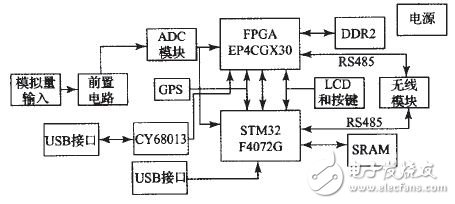
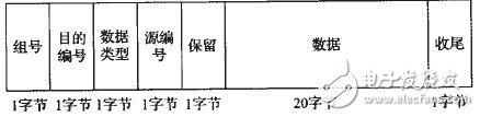
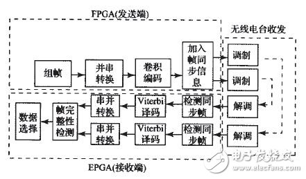
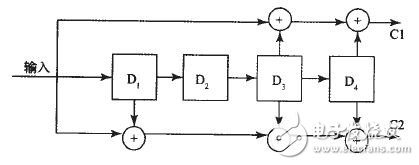
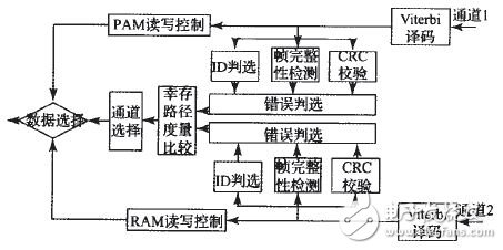
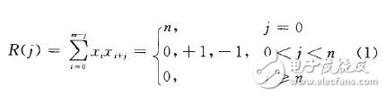
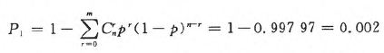
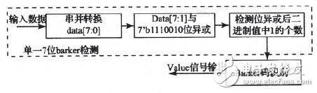
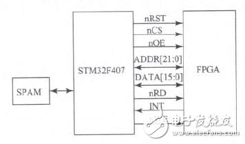
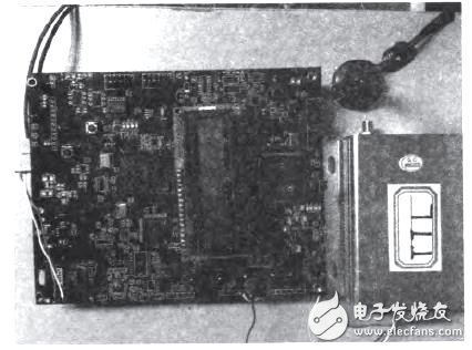
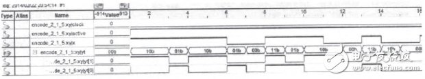
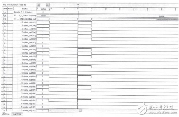
1 Introduction In recent years, with the development of electronic technology, the development of wireless communication technology and computer networks, distributed wireless data acquisition network technology has begun to emerge and is rapidly applied to various fields. In some cases where the terrain is complex and the area that is not suitable for humans needs to be collected, the wireless distributed acquisition can be appropriately selected. In the existing wireless distributed acquisition system, a single chip, a DSP, etc. are often used as the main control unit of the system. However, due to its own working characteristics, it is often weaker than FPGA for accurate timing control and parallel processing capability. With the development of programmable logic devices such as FPGAs, it provides a good implementation platform for reliable transmission of wireless data. Using FPGA as the processor for timing control and signal processing will make the system circuit design more concise, reliable and flexible, which can effectively shorten the development cycle and reduce the development cost. To this end, based on CycloneIV+STM32, a new wireless distributed acquisition system is designed to achieve high reliability and synchronous transmission of data. The design is mainly composed of three parts: encoder, decoder, wireless transceiver station. After the encoder and the decoder are synchronously calibrated, the data to be transmitted is convolutionally encoded and converted into serial data. After the data is converted into serial data, the Barker code is added to the serial data frame header to achieve frame synchronization, and data is simultaneously transmitted using two data transfer channels that are mutually backed up. After the barker code is detected at the data receiving end, the two-channel data that is mutually backed up is viterbi decoded locally (the viterbi decoder designed in this paper adopts a parallel structure, which greatly reduces the decoding time). After the decoding is finished, the local dual-channel data is cyclically redundantly verified, and a decision is made, and finally the corresponding instruction is executed. And the corresponding feedback signal is given at the specified time. The designed wireless acquisition system can effectively recover data and perform reliable data transmission even if a small number of error codes appear in a certain data channel. The monitoring module is added to the system to back up the uploaded data and monitor it in real time. If it is found that it cannot be uploaded normally, the standby module is enabled to ensure the normal operation of the entire system. The system can not only achieve high reliability and synchronous transmission of data, but also has good applicability and can be widely used in the industry. 2 Introduction to Wireless Distributed Acquisition System 2.1 System Hardware Introduction The wireless distributed acquisition system includes an encoder, a decoder (the encoder, the decoder hardware are identical, but the configuration logic is different, and can be configured as an encoder, a decoder, a relay station) and a wireless communication station. As shown in Figure 1, this is the simplest one-to-one distributed system. Figure 1 Wireless distributed acquisition system structure The encoder acts as a bridge between the host computer and the decoder, and transmits and receives commands and data through the USB/RS485 channel. The decoder receives commands from the encoder for configuration and acquisition, and stores the data in DDR2. After receiving the upload command, the decoder uploads the data to the encoder. The block diagram of the encoder/decoder hardware system is shown in Figure 2. The main control unit of this system is completed by FPGA. The FPGA uses Altera's EP4CGX30F407, with logic units of 29,440, 80 18 & TImes; 18 multipliers, and up to 290 user-defined IOs. STM32 basic architecture and standby units monitor the system, series is based STM32F407ZG ARM CortexTM-M4F high performance 32-bit RISC core, the operating frequency up to 168 MHz, the embedded memory STM32F407ZG series of high-speed (up to 1 MB flash memory, Up to 192 KB of SRAM) with three 12-bit ADCs, two DACs, one low-power RTC, 12 general-purpose 16-bit timers, and two general-purpose 32-bit timers. The human-computer interaction part is composed of a 16X2 liquid crystal display character module and four buttons. Its main function is to set the base station number by button and display it on the LCD. The wireless module uses the WSN-03 series wireless module as the transceiver platform, and the working voltage is 5 V. The transmission rate and working frequency band can be configured. Current transmission rates up to 115 200b ps, 433 MHz operating frequency is adjustable. The wireless module and the FPGA are mainly connected by RXD/A, TXD/B, NRST (reset control), SET (set module parameter), and SLP (sleep control) signal lines. The GPS module uses VKl6U6 for positioning, and the FPGA is connected by UART interface, and the baud rate is positioned at 9600 bps. ADC based on the selected 32 bits precision low-power D conversion chip ADSl282 â–³ -Σ technique, the sampled signal level range: a differential input 2.5 ~ + 2.5 V. A single decoder has 6 acquisition channels, which are calculated at a sampling rate of 2 k at a sampling rate of 6 s. The pure data volume of a single decoder is 6 & TImes; 2 k & TImes; 16 & TImes; 24-6144 Kbits. Considering the encoder, one sampling The data of the 8 base stations is 98 304 Kbits after encoding, so the encoder and decoder need to add 1 piece of Micron Technology's MT47H256M8HG-37E IT (256Meg×8) as the buffer space. Since DDR2 SDRAM requires specific control read and write timing, the system directly uses the "DDR2 SDRAM High-Performance Controller" IP CORE that comes with the Quartus II. The USB part consists of two channels, one consisting of FPGA, CY7C68013 and USB interface; the other consists of STM32 (with USB drive) and USB interface. At the same time, RS485 serial port is added in the design, so that the whole system can maintain real-time communication with the host computer, which provides the possibility of remote control of the system and can keep the system updated. Figure 2 system framework 2.2 System Data Flow The data flow of the system is: synchronous calibration decoder, setting the delay after each decoder receives the command-encoder configuration acquisition parameters, command-decoder acquisition data is saved to DDR2, each decoder receives time-sharing data Upload the command and upload the data - the encoder saves the data to the DDR2 data collection and uploads it to the host computer via USB/RS485. The decoder node cooperates with the computer to perform polling collection of data at various points, and includes a wireless transmission module and a USB interface for communicating with the computer. The STM32 backs up the framing data and monitors the FPGA in real time. If it does not work as specified at the specified time, the STM32 will replace the FPGA and put the FPGA into a power-down state. 2.3 System framing format There is a one-to-many relationship between the encoder and the decoder. The decoder uploads data in a time-sharing manner. The decoder has two channels, and the decoder has a unique configuration number. The format of the data frame is shown in Figure 3. In addition to the 20-byte valid data in the data frame, the group number, the destination number, and the like are also included. Figure 3 Encoder, decoder data frame format In order to improve the received signal quality, the system introduces a channel coding method to improve channel quality. Specifically, as shown in Figure 4. The transmitting end performs framing, parallel conversion, convolutional coding, and synchronization frame information on the data, and then transmits the data to the wireless communication station for modulation. The wireless communication station at the receiving end demodulates the signal and sends the data to the FPGA at the receiving end. After receiving the frame synchronization information, the FPGA at the receiving end saves the next data and performs Viterbi decoding. The FPGA performs redundancy check on the dual channel data and selects the correct data to perform related operations. Figure 4 wireless data transmission 3 Implementation of data transmission in wireless distributed acquisition system 3.1 Reliability The data to be transmitted is convolutionally encoded, and the dual channel transmission, Viterbi decoding, redundancy check, and data selection are mutually performed, and the system can perform wireless transmission and reception very well. 3.1.1 Convolutional coding After the data group frame is completed, the low-order to high-order side-by-string conversion is performed to perform convolutional coding. Convolutional coding is an error correction channel coding, which is a coded sequence port that is continuously output after being encoded by successive input information sequences. The convolutional code is described by (n, k, m), k is the number of bits input to the convolutional encoder each time, and the convolutional code corresponding to the k-coded codeword is output as an n-tuple codeword, and m is an encoding. Storage. The n-gram element generated by the convolutional coding is not only related to the current input, but also related to the k-tuple of the previous m-one input. This system uses a (2, 1, 4) convolutional encoder, as shown in Figure 5. The "+" in the figure represents the exclusive OR. Each bit is encoded with 2 bit outputs (C1, C2). Figure 5 (2, 1, 4) convolutional encoder 3.1.2 Viterbi decoding There are two receiving channels at the receiving end, which do not interfere with each other. The receiving end decodes two channels simultaneously. The decoding uses Viterbi decoding. The Viterbi decoding algorithm is a decoding algorithm for convolutional codes. Viterbi decoding can achieve the best decoding according to the maximum likelihood algorithm rule, especially suitable for forward error correction. Taking this design as an example, according to Fig. 5, the four delay states (0, 1) of the encoder constitute 16 states (D4D3D2D1) of the entire encoder, and each state jumps to another when the encoder inputs 1 or 0. a state. And the output changes accordingly. Decoding is the inverse of coding. The algorithm stipulates that the data received at any time t must be subjected to 32 path value calculations and 16 times of comparison. After comparison, only one path value is saved for each state, and the calculation amount is reduced by half for the next calculation. Repeat 208 times, select one of the 16 surviving paths with the smallest path value, and push back this path to get the corresponding decoding output. Considering that after each decoding, the decoder can return to the initial state, so the source data is finally added with 8 bits of "0". This design uses a parallel processing structure to restore the source code after 214 cycles. When designing FPGA logic, basically adopt multiple parallel pipeline technologies, and the decoding part includes four sub-modules: a ratio selection module, a backtracking module, a storage module, and a clock control module. The calculation and comparison of the path values ​​are completed in 3 clock cycles, and 4 modules are simultaneously operated, which greatly reduces the decoding time. In addition, in order to improve the efficiency of the FPGA, the system adds a sampling trigger signal to ensure stable operation of the logic. 3.1.3 Data selection After decoding, the receiving end has received two sets of data that are backed up each other. It has been proved by practice that simple parallel redundancy can greatly improve the reliability of the system. The specific selection process is shown in Figure 6. After two channels of data are decoded by Viterbi, one frame of data is received and written into the RAM, and the CRC check, frame integrity check, and ID are calculated locally. When there is no problem with the above detection, the metric values ​​of the 2-way surviving path are compared, and the channel with the smaller value is selected as the final data. Figure 6 Data selection 3.2 Synchronization implementation In order to ensure strict synchronization between the encoder and the decoder, the data frame needs to be added to the synchronization frame. There are two methods for implementing frame synchronization: start-stop synchronization and centralized insertion synchronization. Start-stop synchronization is relatively simple, and specific start and stop pulses are typically added at the beginning and end of the data symbol to indicate the beginning and end of the data frame. The synchronization code inserted in the centralized plug-in synchronization method requires that the probability of pseudo-synchronization occurring at the receiving end for synchronization recognition is as low as possible, and the code is required to have a sharp autocorrelation property for identification. The 7-bit Barker code is used as the frame synchronization code, and its local autocorrelation function is: It can be seen from the above formula that the autocorrelation function of the 7-bit Barker code has a sharp single-peak characteristic at j_0. In the design, two sets of sync frame headers are used as the sync code, and the sync frame header is composed of 7-bit Barker code and 1 bit of 0. Up to now, the number of bits to be transmitted is 208 × 2 + 8 × 2 - 42 bits. After modulation and demodulation, the receiving end detects frame synchronization information, and the synchronization information is composed of two groups of 11100100. The high 7 bits of each set of synchronization information allows the number of errors to be within 1 bit compared to the 7-bit Barker code. Let P be the symbol error probability, the number of symbols of the behavioral synchronization code group, and m be the maximum number of error symbols in the allowed code group. In the system, row n=7, m=1. At P = 0.01, the probability of leakage synchronization for a single barker code is: When both sets of sync frames are satisfied, frame synchronization is established, and the receiver saves the next data. The wireless communication station is connected to the FPGA by rs485. As shown in Figure 7, the FPGA detects whether X is "0". When "0" is detected, the receiving end does not perform bitwise OR operation on the next data X and the corresponding bit of the local Barker code. . When a 1 byte barker code is detected and a bit is within 1 bit, a value pulse is issued. When two value pulses are detected, the synchronization is established and the receiver starts to store the next data. Figure 7 Barler code identification 4 system monitoring module implementation The connection between STM32 and FPGA is shown in Figure 8. Since the communication between ARM and FPGA directly affects the performance of the controller, the design of the parallel bus becomes a very critical issue. The bus may include a chip address bus (ADDR[021]), a data bus (DB[015]), a control bus, a reset signal (nRST), and an interrupt signal line (INT), wherein the control bus includes an enable signal (nOE) Chip select signal (nCS), read signal (nRD), write signal (nWE), the advantage of this is that the FPGA chip is memoryized, that is, STM32 can control the FPGA work by accessing specific addresses, and can work together The reset signal resets the STM32 and the FPGA chip at the same time, avoiding bus competition and risk. Figure 8 STM32 and FPGA connection STM32 and FPGA simultaneously receive commands. After parsing the command, the FPGA should send data within the specified time. When the FH acknowledges the completion of the frame, it sends an INT signal to 黜2 to apply for an interrupt. If the STM32 does not receive the INT signal from the FPGA within the specified time, it will start timing. If the INT signal is not received within the time limit, the STM32 will stop the FPGA power supply and the STM32 will work instead of the FPGA to ensure the stable operation of the whole system. 5 system test The encoder is shown in Figure 9. A pair of code and decoders were built during the test and powered by a 12 V DC power supply. Outgoing data is 208 bits, i.e. 208'b00000000_10010010_01100100_10011001_00100110_01001001_10010010_01100100_10011001_00100110_01001001_10010010_01100100_10011001_00100110_01001001_10010010_01100100_10011001_00100110_01001001_10010010_01100100_10011001_00100111_00111111; FIG. 10 shows a portion of the signal waveform using a test taken after SignalTap II convolutionally encoded output. Where z is serial input data and yt is data output after convolutional coding. After transmitting wireless data, the Viterbi decoding, as shown in FIG simulation graphics, data sent from the encoder to 11 208 bit S, as a part of the data decoding data_out output decoded data bits and low order of transmission of the opposite side. Since the data is transmitted and the high and low bits are interchanged, only the high 27-bit decoding result after Viterbi decoding is intercepted. After many tests, the data transmission is normal, and the system can automatically correct it in the case of a small number of discontinuous error codes. Figure 9 Encoder physical Figure 10 (2, 1, 4) encoder output Figure ll Viterbi decoding output 6 Conclusion In the design of wireless distributed acquisition system, a two-channel transmission scheme based on convolutional coding, Viterbi decoding and mutual backup is adopted. The rich logic resources and storage resources in the FPGA are utilized to realize long-distance synchronization of data. Reliable transmission. After adding the backup data channel, the real-time verification and automatic selection of the two-way data are realized on the hardware through the internal logic control of the FPGA, which improves the stability and reliability of the system. Compared with the mechanism of “backup-retransmissionâ€, the method is simple and real-time. Even if a channel fails to work normally, the system can still perform normally. The wireless distributed acquisition system satisfies the transmission of the current synchronous trigger and the small amount of data. The two-channel codec and data redundancy transmission mechanism proposed in this paper can also be applied to the related wireless transmission field to improve the reliability and stability of long-distance data transmission.
Single-axis Wearable Stabilizer
With a gyro-stabilized gimbal system, the Single-Axis Wearable Stabilizer keeps stabilized or steerable horizon with automatic calibration to give you an unprecedented smooth shooting experience.
Also, it`s wearable on your head, chest, shoulder or on bike and motorbike.
Wewow focusing on handheld stabilizer is a technology company which does R & D independently. With Wenpod series product released, the company achieved the industry's praise and quickly became the leader of the smart stabilizer industry.
If you have any questions, please contact with us directly.
Wewow appreciates domestic and international business relationship!
Single-axis Wearable Stabilizer Single-Axis Wearable Stabilizer,Professional Single-Axis Wearable Stabilizer,Wearable Stabilizer With Single Handheld,Handheld Single-Axis Wearable Stabilizer GUANGZHOU WEWOW ELECTRONIC CO., LTD. , https://www.stabilizers.pl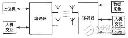


Our service
1. Reply to you within 24 hours.
2. Already sample: within 1-2days.
3. Shipping date: within 24 hours once get the payment.
4. 12 months warranty.
5. After-sales service, solve within 3 working dates.