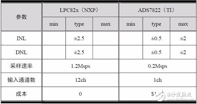
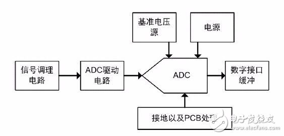
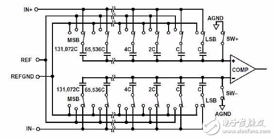
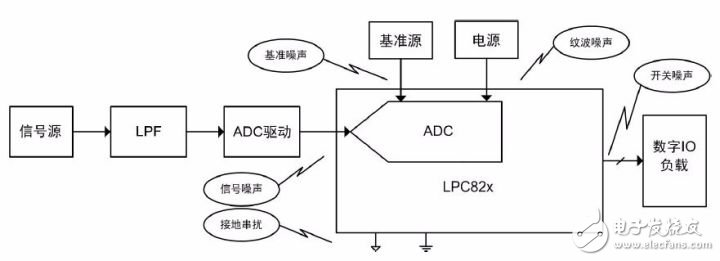
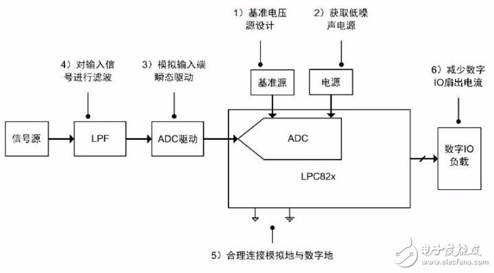
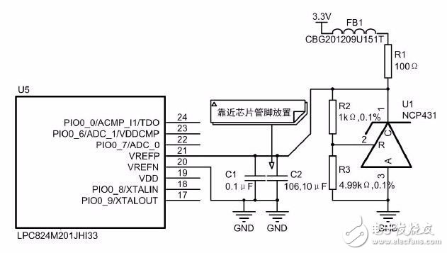
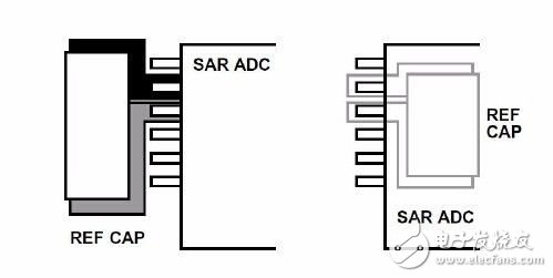
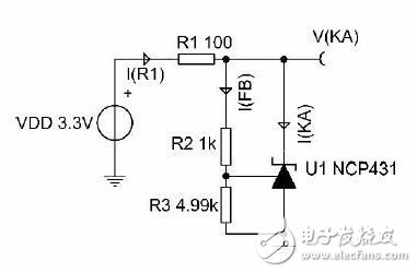
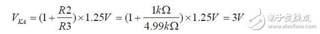
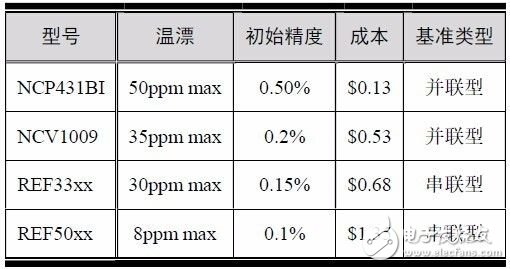
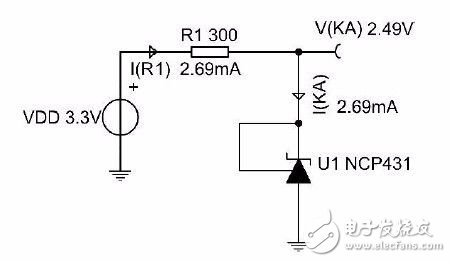
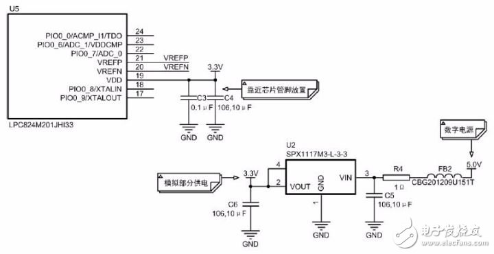
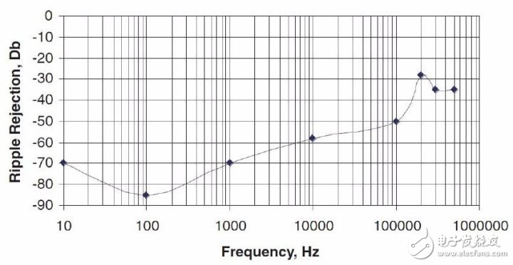
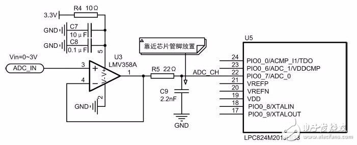
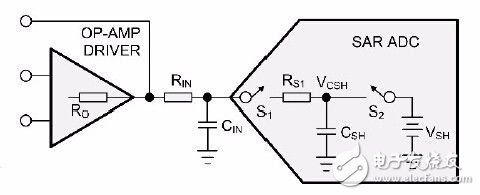
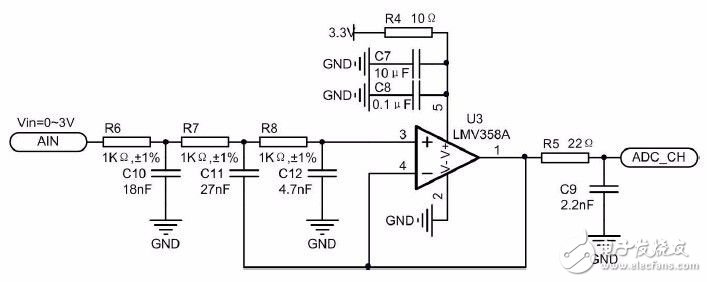
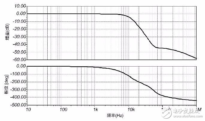
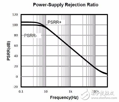
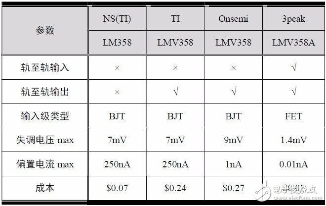
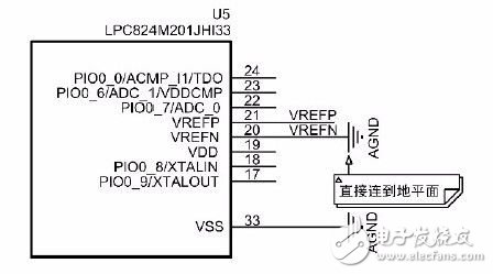
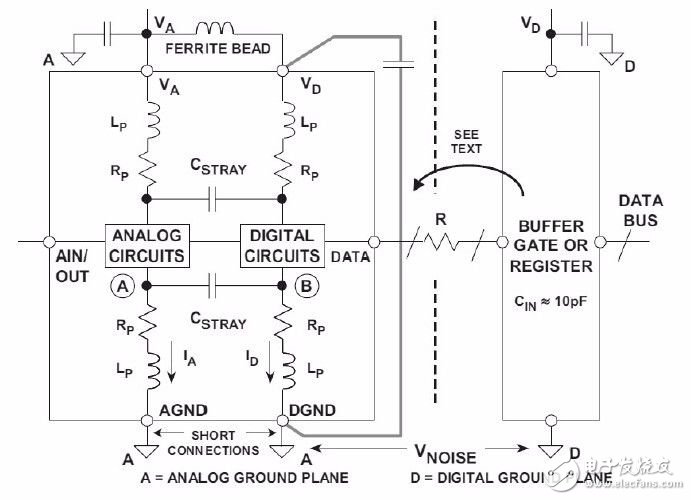
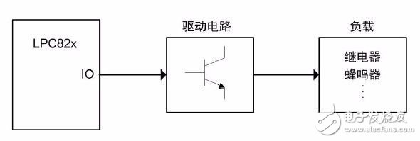
Professor Zhou Ligong's new book, "Programming for AMetal Frameworks and Interfaces (Part 1)", provides an in-depth introduction to the AMetal framework. By reading this book, developers can learn advanced software design principles and development approaches for interface programming. Focusing on your own "core domain," you can change your programming mindset and achieve mutual growth between your company and yourself. Authorized by Professor Zhou Ligong, the Zhiyuan Electronic Public Number will serialize the content of the book, and is committed to sharing it with readers. The second chapter covers ADC signal conditioning circuit design, specifically sections 2.1 application background and 2.2 circuit design. This chapter guides: For developers, designing analog circuits is often one of the most challenging tasks. It not only requires significant investment in equipment but also a high-level instructor with both theoretical knowledge and practical experience to create an analog circuit that meets the required specifications. After analyzing user-designed analog circuits, it was found that most developers have limited understanding of the details involved in analog circuit design. Although many semiconductor companies provide extensive design reference materials, there is still confusion when it comes to certain key points. This is why many developers remain anxious about working with analog circuits. For MCU suppliers, the information provided is typically focused on digital circuit design and basic software. Almost all MCU vendors do not offer valuable references for application circuit design. The information provided by each manufacturer is similar, and it's hard to find something truly useful. In fact, this knowledge is non-core for developers, yet it takes a lot of time to master. Based on this, we have standardized the peripheral circuits required for various ADCs within the MCU, aiming to elevate the overall design level across the industry. While there are differences in every requirement, mastering the correct design methods can lead to consistent results. 2.1 Application Background > > > 2.1.1 Nominal Accuracy The LPC824 features a 12-bit SAR ADC with up to 12 input channels and multiple internal and external trigger inputs, offering a sampling rate of up to 1.2MS/s. Compared to standalone 12-bit ADC chips, the key parameters listed in the manual are very close. In theory, better acquisition accuracy should be achievable. See Table 2.1 for details. However, in practical applications, user test results often fall far short of the nominal values, indicating poor internal ADC accuracy caused by unreasonable external circuit design. Table 2.1 LPC82x Internal ADC Key Parameters > > > 2.1.2 Peripheral Circuit As shown in Figure 2.1, the sampling system using the LPC82x internal ADC requires support from a reference source, power supply, drive circuit, and signal conditioning circuit. These components fundamentally influence the performance of the ADC. Figure 2.1 Peripheral Support Circuitry Required for Internal ADC > > > 2.1.3 Interference Source Most integrated ADCs in MCUs are SAR type due to their switched capacitor structure and ease of implementation in semiconductor processes. However, because they have multiple active input ports, they are susceptible to interference. The internal structure of a typical SAR ADC is shown in Figure 2.2. Understanding its working principle helps identify how interference enters the system. Figure 2.2 SAR ADC Internal Structure The ADC output code is determined in two stages. During the acquisition phase, switches SW+ and SW- are off, and all switches are connected to the IN+ and IN- analog inputs, allowing each capacitor to function as a sampling capacitor. In the conversion phase, SW+ and SW- are turned on, disconnecting the analog input from the internal capacitors. When the capacitors are applied to the comparator input, the comparator becomes unstable. Starting from the MSB, the AR algorithm switches the components of the weighted capacitor array between REF and REFGND, causing the comparator to stabilize, which produces a digital output representing the analog input. During the conversion process, the total power of the input signal is repeatedly distributed across the capacitors in the weight capacitor array. Each bit of conversion data is generated based on comparison with the reference source, determining whether the output code is 0 or 1. Any noise on the reference source directly affects the output code. If there is interference between the power supply and ground during the comparison, the result of the internal comparator changes, indirectly causing instability in the ADC output data bits. See Figure 2.3 for more details. Figure 2.3 SAR ADC has multiple active input ports SAR ADC’s repeated comparison structure means that the reference source, power supply, ground, or digital interface may be connected to interference signals, effectively creating multiple valid input ports, not just one. Preventing external interference signals from being coupled through other pins than the ADC signal input is essential for achieving stable data output. 2.2 Circuit Design Improving the accuracy of the internal SAR ADC involves eliminating interference at each valid input port, as shown in Figure 2.4. Figure 2.4 Method to Eliminate Interference from the ADC Peripheral Support Circuit According to the impact on accuracy, the design of the voltage reference source accounts for 80% of the workload, low-noise analog power supply for 5%, input transient drive for 5%, and other anti-interference measures for 10%. > > > 2.2.1 Reference Source The reference voltage directly affects the digital output of the ADC, requiring low noise, low output impedance, and good temperature stability. The standardized circuit is shown in Figure 2.5. Figure 2.5 Low Noise and Low Output Impedance Reference Voltage Source Circuit In this circuit, C2 and C1 are storage capacitors for the internal ADC reference source pin, R2 and R3 set the output voltage of the NCP431 reference source chip, R1 sets the static operating current of the NCP431, and FB1 and R1 form a low-pass filter with C2 to filter out high-frequency interference from the 3.3V supply. 1. Low Noise and Low Output Impedance The reference voltage chip uses a low-cost NCP431 with an output noise of 10uVpp and an output impedance of 0.2Ω. This noise level is already sufficient for 12-bit precision, but the dynamic output impedance is 0.2Ω. Using the low-frequency impedance of the energy storage or decoupling capacitors C2 and C1 in Figure 2.5, the instantaneous high-frequency current on the reference source pin during ADC conversion can be supplied, effectively solving the high-frequency output impedance issue of the reference source. Note that the 10uF capacitor C2 on the VREF pin is not a bypass capacitor but part of the SAR ADC. This large capacitor is not suitable for placement on silicon. During bit judgment, since each output bit is established in tens of nanoseconds or faster, the storage capacitor is used to supplement the switched capacitor array to balance the comparator with the existing charge on the internal capacitor array. This large-value storage capacitor needs to meet the ADC bit judgment setup time requirement. To reduce its high-frequency ESR, C2 prefers the X5R material chip ceramic capacitor, ensuring it is placed close to the reference source pin VREFP and grounded close to the VREFN analog ground pin, as shown in Figure 2.6. Figure 2.6 How to Place the VREF Pin Storage Capacitor on the Same Side as the Chip 2. Static Operating Current The NCP431 is a shunt-type reference. Its principle is similar to a Zener diode and can only sink current. See Figure 2.7 for details. When the load current is supplied, the voltage across the reference source is maintained, the total current flowing through the current limiting resistor R1 is kept constant, and the quiescent current of the reference source itself is adjusted to decrease, so that the current on the load increases. The value of R1 needs to be calculated to ensure that there is the most residual quiescent current at the maximum load current. Figure 2.7 Parallel Static Operating Current The minimum quiescent current I(KA)min in the NCP431 manual is 1 mA. The NCP output voltage adjustment resistors R2 and R3 sink the current I(FB) to 0.5 mA. The average current I(REF) absorbed by the REF pin of the LPC82x is approximately 100uA, leaving a margin of 1.5mA. The total quiescent current is taken as 3 mA, which determines the resistance of the quiescent operating current R1: 3. Output Voltage Selection According to the LPC82x manual, for best performance, VREFP and VREFN should select the same voltage level as VDD and VSS. If VREFP and VREFN select values other than VDD and VSS, you should ensure that the intermediate values are the same: The actual test found that the reference voltage is set to 3.0V. The accuracy is optimal. If it rises to 3.3V near the LPC82x, the measured value of the INL of the ADC starts to decrease because it is close to the power rail. Therefore, R2 and R3 in the standard circuit will be used for the NCP431. The output voltage is adjusted to this value and is calculated as follows: 4. Temperature Drift and DC Accuracy Temperature drift and initial DC accuracy are inherent parameters of the reference source chip. The lower the temperature drift, the higher the initial accuracy and the higher the cost. Benchmarks with a temperature drift of less than 25 ppm almost exceed the cost of the LPC82x chip itself. See Table 2.2 for details. Table 2.2 Reference Voltage Source Parameters and Costs Considering the NCP431 as a relatively suitable choice, it is an improved version of ONSemi's TL431 with a maximum temperature drift from the original 92 ppm/°C to 50 ppm/°C with an initial accuracy better than 0.5%. Taking 25°C as the reference temperature, the temperature drift value introduces an error of about 0.3% in the range of -40°C to +85°C, which basically conforms to the application of 12-bit ADC acquisition accuracy. It should be noted that R2 and R3 in the standardized circuit affect the temperature drift of the NCP431, and the low temperature drift coefficient of 25 ppm or less should be selected. If you consider cost savings or no optional resistors, use a 2.5V output circuit as shown in Figure 2.8 instead of affecting the reference temperature drift. Figure 2.8 NCP431 Reference Source Circuit Without External Resistor After the reference voltage drops from 3V to 2.5V, it has a slight effect on the INL of the LPC82x internal ADC. > > > 2.2.2 Low Noise Analog Power Supply To avoid interference from the power port, a low-noise power supply is required. Using the ripple rejection ratio of the linear regulator, this low noise power supply can be obtained from a typical digital ambient switching power supply, as shown in Figure 2.9. Figure 2.9 Low Noise Analog Power Circuit Using the passive filter network composed of FB2, R4, and C5, the problem of the ripple rejection ratio of 1117 in the high frequency band can be effectively improved, and the ripple noise suppression from low frequency to high frequency can be realized. Among them, R3 and C5 form a low-pass filter with a cutoff frequency of 1.59KHz, which makes the ripple interference of the switching power supply above 100kHz common on the 3.3V power supply more than 10dB. Bead FB2 exhibits high impedance at high frequencies, combined with C5's low-pass filter at higher frequencies to form a higher attenuation factor, effectively filtering out spike glitch noise on the 3.3V supply. The linear regulator uses the SPX1117. The ripple rejection ratio curve is shown in Figure 2.10. It has a good ripple rejection ratio of -60dB in the low frequency to 10kHz band and a fast drop after 100kHz. Figure 2.10 Ripple Rejection Ratio of SPX1117 The linear regulator U2 should be placed close to the LPC82x. Other digital circuits do not share the 3.3V power supply of the MCU. If the cost is shared, the digital part of the power supply is isolated by the LC filter circuit. > > > 2.2.3 Transient Drive The SAR ADC input has an instantaneous charging process during sampling. If the signal source impedance and the internal sampling capacitor are not properly handled, the best output is not available in the microprocessor or in the external ADC. Precision. The operational amplifier and RC combination circuit used in the standardized circuit is shown in Figure 2.11. Figure 2.11 Internal ADC Input Transient Drive Circuit Understanding the transient drive circuit through the equivalent circuit of the typical SAR ADC input. As shown in Figure 2.12, the input is equivalent to a switch S1 connected to a capacitor C SH connected to ground. Before voltage sampling, the sampling capacitor C SH is connected to the power supply, voltage reference or ground through switch S2 for pre-charging. The value is determined by the internal circuitry of the ADC. At the beginning of the voltage sampling, S2 turns on S1 to close. Figure 2.12 SAR Type ADC Input Equivalent Circuit When S1 is closed, the drive circuit from electric charge injected or aspirated C SH, the ADC needs some time to sample the signal. During this sampling time, the ADC needs to draw enough charge from the driver circuit to C SH to make the system within 1/2-LSB accuracy. If the signal source impedance R O is too large, the time constant of the RC network composed of R O , R s1RS1 , and C SH is too large, resulting in insufficient voltage settling time on C SH during the sampling time, and the collected voltage value will decrease. A better solution is shown in Figure 2.12. Adding an op amp buffer reduces the internal resistance of the signal source. No matter whether the source impedance R O is high or low, the accuracy will not be affected. When the op amp is used directly to drive the ADC input, the charging current at the instant of S1 closing will interfere with the output voltage of the op amp, resulting in inaccurate ADC output. In order to achieve higher circuit accuracy of the design, a resistor R in capacitor C in is added between the op amp and the ADC. C in is used as a charge memory to supply enough charge to the input of the ADC at the sampling instant, and R In is used to prevent the op amp from driving capacitive loads, making the op amp work more stable. > > > 2.2.4 Input Signal Filtering The input signal itself may contain undesired interference signals, and adding a filter to the input circuit to suppress interference is a necessary hardware anti-interference measure. If the interference is filtered by the post-data processing of the sampled data, according to the sampling theorem, an anti-aliasing filter must be set on the hardware to limit the input signal bandwidth to below the 1/2 sampling frequency. Active Filter The ADC-operated op amp is multiplexed in the standardized circuit to implement a third-order active low-pass filter, as shown in Figure 2.13. Figure 2.13 Third-order Low-pass Active Filter The low-pass cutoff frequency of the filter is set to 9 kHz and the type is third-order Bessel with good attenuation characteristics. And using the 3rd-order circuit form in Figure 2.13, the second-order Sallen-Key filter topology is avoided by the conventional single op amp, and the high-frequency feedthrough problem occurs due to insufficient bandwidth of the op amp. Even if the LMV358A is not used, the high-frequency signal penetration filter will not appear. See Figure 2.14 for details. Figure 2.14 Frequency Response of the Third-order Filter 2. Resistance Noise and Power Supply Rejection Ratio of the Op Amp In general, the active filter itself may generate noise, commonly referred to as device noise, which is the thermal noise of the resistor and the voltage output noise of the op amp. The greater the resistance value, the greater the resistance noise introduced. The Johnson noise of a 1kΩ resistor is approximately 4nV/(Hz) 1/2, which varies with the square root of the resistor. If resistance noise is taken into account, the recommended resistance is 1~10kΩ. The resistance noise can be filtered out in the filter circuit that can be attributed to it, but it and the op amp output noise are the source of the noise generated in the circuit. It should be considered in the design, and the low resistance value and low noise op amp should be properly used. In addition, the power supply rejection ratio of the op amp should be considered. The noise on the power supply is conducted to the signal path with the power supply pin of each active device. As an op amp for the ADC driver amplifier, its own power supply rejection ratio is superimposed on the op amp if the noise is not suppressed. In the output. In particular, when a switching power supply is used in a circuit, there is a high-frequency spike voltage noise on the power supply, and the power supply rejection of the operational amplifier generally drops sharply at a high frequency, and does not inhibit them. Taking the op amp LMV358A used in the standard circuit diagram as an example, the power supply rejection ratio is shown in Figure 2.15. Figure 2.15 LMV358A Power Supply Rejection Ratio A simple way to solve this problem is to use an RC low-pass filter to filter the op amp power supply and filter out the high-frequency components whose power supply rejection is low, as shown in Figure 2.13 for R4 and C7. If the power supply terminal of the op amp is regarded as high impedance (its operating current is small), the cutoff frequency of the RC filter is about 1.6 kHz, which can effectively attenuate the high frequency interference signal. 3. Op Amp Selection Acquisition applications using the LPC82x internal ADC typically impose stringent device cost requirements, and standardized circuit design considers the lowest cost op amp – the LM358 series. Classic op amp devices usually have two problems. The input and output signal range cannot reach the power supply voltage under single power supply condition (the input and output cannot be rail-to-rail), the signal measurement range is narrow; the input offset voltage and bias current are relatively large, and the DC accuracy is affected. Large, so can't be used. However, many manufacturers have already produced LM358 compatible or improved products, as shown in Table 2.3. Table 2.3 Selection of Low-cost Op Amp Parameters The data in the table shows that only 3peak's improved device LMV358A supports both rail-to-rail input and output, FET input stage and low offset voltage, and the cost is consistent with the original LM358, which can meet the application requirements, so the standardized circuit finally chooses LMV358A. > > > 2.2.5 Analog Ground and Digital Ground An MCU with an internal ADC typically has a separate AGND pin and a normal GND pin. How to connect AGND to GND is often unclear, and the optimal design method to avoid mutual interference is that the AGND and GND pins are all connected to the ground plane, as shown in Figure 2.16. Figure 2.16 Connection Between AGND and GND Understanding the ground pin structure inside the mixed-signal IC helps to understand the intent of the IC to set the analog ground and digital ground pins. See Figure 2.17 for details. Keeping the ground pin independent can avoid coupling digital signals into the analog circuitry. Inside the IC, the bond wire connecting the silicon pad to the package pin will inevitably produce wire bonding inductance L P LP and resistor R P RP , which IC designers can't do. If the ground pin is shared, the rapidly changing digital current generates a voltage at point B, which is unacceptable for the analog circuit, and the IC designer intends to separate the ground pin to eliminate this effect. Figure 2.17 IC Internal Analog and Digital Ground Connection However, after the separation, the voltage at point B is also coupled to point A of the analog circuit through the stray capacitance C STRAY CSTRAY . Approximately 0.2 pF of parasitic capacitance between each pin of the IC package is unavoidable. To prevent further coupling, AGND and DGND should be tied together externally via the shortest leads and connected to the analog ground plane. Any additional impedance within the DGND connection will generate more digital noise at point B; this in turn causes more digital noise to be coupled to the analog circuit through the stray capacitance. > > > 2.2.6 I/O Fanout Current Since the LPC82x has only one power supply pin, the MCU digital power supply is shared with the internal ADC analog power supply. Although this design can provide as many I/O ports as possible in a small package, it will cause interference problems in the analog part: the MCU generates digital switching current on the power supply, generates noise voltage through the shared pin, and interferes with the internal ADC. The following optimization suggestions can largely avoid interference: Avoid direct driving of large currents on the I/O port, indirect drive using a triode or logic chip, as shown in Figure 2.18; If conditions permit, switch to low power mode to perform ADC acquisition. Figure 2.18 Using the Driver Circuit to Reduce I/O Fanout D-subminiature Connector,D-Sub Connector,Power D-Sub,D-Sub Power Connector,High Power D-Sub Connector,db9,db15,db25,ip67 D-Sub,waterproof D-Sub connector,D-Sub connector female,D-Sub male connector Dongguan Yiyou Electronic Technology Co., Ltd. , https://www.dsubminiature.com