The wireless communication market has been steadily shifting towards cost-effective, low-power, and compact solutions. Short-range devices are increasingly driving the demand for radio frequency (RF) integrated circuits (ICs), especially through the concept of wireless sensor networks. RF transceivers are specifically designed to minimize power consumption, with low-voltage operation being a key requirement. However, this creates a significant challenge between achieving high performance and maintaining low power usage. In recent years, the development of RF IC technology has advanced rapidly, with high-speed and low-power components becoming central to industry focus. The current 0.13µm RF CMOS transistor, for instance, has an fT value of up to 60 GHz, indicating that CMOS technology is now capable of handling high-frequency signals. As a result, RF CMOS has become the dominant platform for the design and optimization of low-power RF ICs.
This article provides an overview of the design of an ultra-low power CMOS radio frequency chip, focusing on the 2.4GHz IEEE 802.15.4 RF transceiver used in Zigbee and RF4CE standards. It explores the design from both a circuit and system perspective, highlighting the key considerations in chip design and application. These include compliance with communication standards and understanding the behavior of the circuit. On the receiving side, the process begins with the antenna capturing the 2.4GHz RF signal, which is then amplified by the Low Noise Amplifier (LNA), followed by mixing, filtering, limiting, and RSSI measurement before reaching the digital demodulator and storing data in the RX-FIFO. On the transmit side, data from the TX-FIFO is modulated using a Voltage-Controlled Oscillator (VCO) and two-point delta-sigma modulation, then amplified by the Power Amplifier (PA) and transmitted via the antenna. The article also discusses hardware design priorities for the antenna and PCB, along with software control, to help readers understand how to implement low-power Zigbee or RF4CE networks using the A7153.
**Zigbee Modulation and PA Design Considerations**
The 2.4GHz Zigbee standard specifies a 250kbps spread spectrum (DSSS) transmission rate and employs Offset-QPSK with half-sine pulse shaping, which is equivalent to Minimum Shift Keying (MSK). Unlike phase shift keying (PSK) or orthogonal frequency division multiplexing (OFDM), MSK is a constant envelope modulation technique, offering higher efficiency but lower linearity. This makes it ideal for power amplifiers aimed at reducing TX power consumption.
**TX Transmitter Design Considerations**
In digital modulation systems, IQ modulation is a common approach. It splits the data into I and Q components, converts them into analog signals using DACs and half-sine pulse shaping, and then up-converts them to RF using a quadrature mixer. While this method allows for precise modulation indices, it requires more complex circuitry. Alternatively, since Zigbee’s modulation is equivalent to MSK, which is a form of FSK, a VCO can be used to directly control the frequency without requiring mixers. There are two types of VCO-based modulation: open-loop and closed-loop. Open-loop systems offer lower power consumption but suffer from frequency drift due to lack of locking. Closed-loop systems, typically using delta-sigma modulation, lock the VCO frequency via a PLL, eliminating drift but introducing limitations in loop bandwidth. For higher data rates, a two-point delta-sigma modulation can be employed, combining differential integration and VCO modulation to achieve full data modulation.
It's important to note that the voltage-to-frequency curve of the VCO can vary with manufacturing processes, so correction circuits are often needed. A linear VCO response can significantly simplify these corrections.
**RX Receiver Design Considerations**
Zero-IF and Low-IF architectures are commonly used in integrated receiver designs. Zero-IF receivers down-convert the RF signal directly to baseband, digitize it with an ADC, and demodulate using a DSP. They benefit from simple low-pass filters, but face issues like DC offset and flicker noise. Additional circuits are required to mitigate these, increasing power consumption. Low-IF receivers reduce the RF signal to a low intermediate frequency, which helps reduce DC offset and flicker noise but introduces image interference. To address this, they require image rejection filters and band-pass filters, leading to higher Q values and increased power consumption.
ZGAR PCC
ZGAR PCC
ZGAR electronic cigarette uses high-tech R&D, food grade disposable pod device and high-quality raw material. All package designs are Original IP. Our designer team is from Hong Kong. We have very high requirements for product quality, flavors taste and packaging design. The E-liquid is imported, materials are food grade, and assembly plant is medical-grade dust-free workshops.
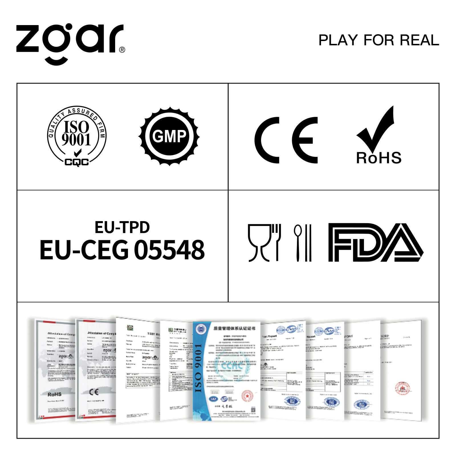
From production to packaging, the whole system of tracking, efficient and orderly process, achieving daily efficient output. We pay attention to the details of each process control. The first class dust-free production workshop has passed the GMP food and drug production standard certification, ensuring quality and safety. We choose the products with a traceability system, which can not only effectively track and trace all kinds of data, but also ensure good product quality.
We offer best price, high quality Vape Device, E-Cigarette Vape Pen, Disposable Device Vape,Vape Pen Atomizer, Electronic cigarette to all over the world.
Much Better Vaping Experience!


ZGAR PCC E-Cigarette Vape Pen,ZGAR PCC Device Vape,ZGAR PCC Vape Pen Atomizer,Latest Disposable E-Cigarette OEM vape pen,ZGAR PCC electronic cigarette
Zgar International (M) SDN BHD , https://www.zgarvape.com

