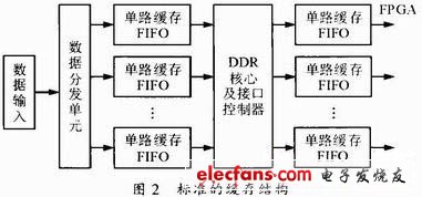
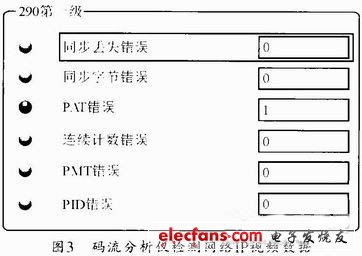
With the continuous development of high-speed processors, the application fields of embedded systems are becoming more and more extensive. High-speed large-capacity buffers are widely used in audio and video systems. However, the price of dedicated high-speed large-capacity cache chips is too expensive, and traditional SDRAM is in bandwidth. It has gradually been unable to meet the application requirements, especially for multi-channel data multi-input and multi-output, neither of which can meet the requirements very well. Here we propose a design that uses double-edge random dynamic memory (DDR SDRAM) combined with additional dedicated circuits Program. It is designed and applied in EOAM modulator system based on DVB-C. The basic requirement of this system is to be able to buffer Gigabit IP data of multiple video TS streams and distribute IP data in multiple channels at high speed; the input is 2 gigabit networks. Port, hundreds of data distribution channels output to the RF interface. In the past system design, some people proposed to use ordinary SDRAM chips as physical cache units. However, due to the limitation of the working speed of such chips, under the condition of basic bit width, the high bandwidth requirements of the above system cannot be achieved. If you do not increase the chip speed, simply increase the bit width, because the delay of each data is different, and the 3.3 V voltage used by SDRAM has a wide transition between the rising and falling edges, it will cause the chip data sampling time window to narrow, and the data transmission reliability Decrease; At the same time, as the bit width increases, the number of pins increases, resulting in a linear increase in design complexity. In this paper, DDR SDRAM is used as a storage unit. Without changing the system clock, the clock double-edge is used to transmit data, and the transmission bandwidth of the chip with the same frequency is doubled on the basis of SDRAM, which satisfies the needs of high-bandwidth cache. . 1 Introduction to DDR memory DDR memory is double data rate synchronous dynamic random access memory. It is the same as the early single data rate synchronous dynamic random access memory. The internal storage unit uses capacitor charging to save data, so the capacitor must be constantly charged to maintain data. This is called "Refresh". The SDRAM data bus accesses data at the rising edge of each clock, while DDR SDRAM accesses data at the rising and falling edges of each clock, so that the data bus width and clock frequency remain unchanged Under the conditions, the data bus bandwidth has been doubled. 2 System design The design uses Xilinx's Sptan3a-dsp 1800a as the main controller, and uses Micron's MT64V32X16 chip as the storage medium, with a maximum storage capacity of 512M. The logical part of the system consists of the arbitration module, input cache module, scheduling decision module, address conversion module And DDR interface control module and other parts, the structural block diagram is shown in Figure 1. The arbitration module in the core controller generates corresponding control commands. Complete the initialization and reset after power-on, and in the process of system operation, issue refresh instructions, write operation instructions and read operation instructions according to the work priority; the DDR interface control module implements the core controller instructions according to the basic timing of DDR chip operation For the information transmission of the physical chip; the Nanyu DDR chip has a non-real-time operation characteristic, and the internal input buffer RAM must be used for basic real-time data buffering; the address conversion module and the scheduling decision module cooperate with the internal input buffer RAM to complete the DDR chip Mapping of internal storage space. 3 DDR core controller design DDR memory is a high-speed memory chip with relatively complex instructions. It must be initialized after power-on to perform other operations; it does not support single-cycle read and write operations, and only supports burst read and write operations with cycles of 4, 4, and 8. In addition, due to its capacitance characteristics, DDR chips are unstable in data storage, and need to be refreshed within a certain period of time to ensure that data will not be lost. Therefore, there are dozens of instructions during the DDR operation. But in this design, the DDR interface controller uses the DDR IP provided by Xilinx, so that the arbitration module in the core controller only needs to use 4 instructions such as idle, initialization, read operation and write operation to complete the DDR-SDRAM. Operation, greatly reducing the design difficulty. Because the design goal is to eliminate the jitter from the network to the IP data, and ultimately to distribute the IP data to 512 channels, which greatly exceeds the previous design's use of DDR, so this article proposes the design shown in Figure 1 here, you can complete Design and application of DDR memory to high-speed large-capacity multi-channel: (1) Input cache module The input buffer consists of a RAM plus external logic circuits, which buffers the TS packet payload that has been input but has not had time to write to the DDR. After the arbitration module sends a signal to allow writing, the data packet in the input buffer is passed to the arbitration module, and the corresponding storage space is released. According to the working mode of DDR and the characteristics of DVB-C, the data transmission of the input buffer takes TS packets as a unit to realize continuous burst transmission of 192 bytes. (2) Scheduling decision module The scheduling decision module receives the read request queue information and implements the decision to dispatch the FIFO with the largest amount of data in the same bank out of the queue when reading data. This module saves the current number of data packets in each channel FIFO. (3) Address conversion module The address conversion module is responsible for mapping the channel number and the internal storage space of the DDR SDRAM chip. The variables saved in this module include the block start address, block end address, FIFO head offset and FIFO tail offset of each channel in DDR SDRAM. (4) Arbitration module The arbitration module generates corresponding control commands, and issues idle commands, initialization commands, write operation commands, and read operation commands according to the work priority. 4 Improvement of resource consumption structure 4.1 Standard MIMO structure buffer For the multi-channel data cache, a multi-input and multi-output buffer structure is designed. The data stream input from the physical channel is first identified and distributed. An input buffer FIFO and an output buffer FIFO are configured for each program stream. The structure is shown in Figure 2. As shown. The advantage of this structure is that there is a separate cache space for each channel of the program, and each channel of the program is relatively independent and does not interfere with each other; when the number of program channels is small, the structure is more efficient and convenient Expand. However, the problem with the above structure is that if there are too many program channels and the input data flow is too large, the number of FPGA internal buffers will increase geometrically, which greatly consumes FPGA resources, reduces the operating clock frequency, and causes the system speed to decrease after synthesis. 4.2 MIMO structure buffer with fixed port Due to the problems of the standard MIMO structure, it is difficult to meet the application requirements required in this article, so there is an improved design proposed here. This design does not cache the DDR on the logical structure like standard MIMO, but uses the physical structure to cache the fast storage by fixing the DDR high-order address, as shown in Figure 1. In this structure, the external stream processing module first distributes the data stream and the channel number stored in the data stream to the cache RAM and the address conversion module, and then the scheduling module schedules the converted corresponding address pointer and sends it to the DDR for correspondence The physical storage space and the output port are only targeted at the physical output port in the same way, which requires a read request queue to send the destination channel to be read in advance. Here the scheduling module can detect the usage of each channel in real time and quickly distribute the data stream. This structure can greatly reduce the consumption of RAM in the FPGA for EQAM, a device that inputs hundreds of streams to a physical IP port, and has a small impact on DDR. It does not reduce system performance too much. Moreover, using RAM directly in the front-end data cache instead of FIFO is more conducive to synchronizing the data stream and the corresponding address. 5 System test In order to test the reliability of this design, after embedding the above-mentioned modules in the EQAM system, the IP video data from the network was received, and after checking the data results through the code stream analyzer, it was found that the data stream packet counter was not wrong after the DDR buffer, and there was no loss. In the case of packets, the stream analyzer comes with a player that can clearly and continuously play the festival, as shown in Figure 3. However, during the program conversion process, a PAT error may occur due to different programs. This error does not affect the normal playback of the program. 6 Conclusion This paper presents an improved MIMO structure DDR buffer, and describes the core control module implementation function, and discusses the impact of the improved design on the system. The final test results also show that this design can be applied to the cache of multi-channel large-capacity video equipment.
Features:
Ideal for entrance ways to parties, adding some refreshing ambiance to your special occasion, creating the ultimate sparkle for
your event, or make a statement at the entrance to your wedding marquee.
A perfect decoration for Valentine's Day, Christmas, other Holidays, Garden, Party, Wedding, Mall, etc.
These LED net mesh light have a very long life expectancy.
Super bright and low power consumption Led Net Lights,Outdoor Led Net Lights,Christmas Led Net Lights,White Led Net Lights XINGYONG XMAS OPTICAL (DONGGUAN ) CO., LTD , https://www.xingyongxmas.com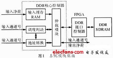
Durable and waterproof for both indoor and outdoor decoration
This Mesh LED is perfect decoration for curtain,room, garden, home, restaurants or bar, wedding, birthday party, Christmas and any other happy events.
8 different modes of glimmering:
Combination, In waves, Sequential, Slo-Glo, Chasing/Flash, Slow fade, Twinkle/flash and Steady on